

 Printed Circuit Boards
 Surface
 PCB Assembly
 Layer Buildup
 Online Tools
 PCB Design-Aid & Layout
 Mechanics
 SMD-Stencils
 Quality
 Drills & Throughplating
 Factory & Certificate


- manufacturing<\/a> cost goes to be maximum. Along with that, the following methods to distinguish between the three-layer board and six layers can be:<\/p>\r\n\r\n<ul>\r\n\t<li>Checking the board through the holes present in the board:<\/li>\r\n<\/ul>\r\n\r\n<p>If there is the presence of through holes only in the front part, not in the back, it notifies a 6-layer PCB board. Otherwise, it might be a 3-layer PCB of 4 layers.<\/p>\r\n\r\n<ul>\r\n\t<li>Checking the wires in the front of the board:<\/li>\r\n<\/ul>\r\n\r\n<p>Since the number of wires in six layers will be more significant than three-layer PCB, it will be more significant. However, on looking for individual layers, the six-layer comprises fewer compact wires than the three layers since it has more prominent space to spread out.<\/p>\r\n\r\n<h3><strong>Pros and cons<\/strong><\/h3>\r\n\r\n<p>The advantages and disadvantages of the 3-layer PCB Vs. 6 layer PCB are mentioned below:<\/p>\r\n\r\n<ul>\r\n\t<li>Since the number of layers is less in 3-layer PCB to 6 layers, it has a cheaper cost and requires less complexity to produce.<\/li>\r\n\t<li>Also, designing the 3-layer PCB is relatively easy compared to the 6-layer board.<\/li>\r\n\t<li>The 3-layer PCB is much more reliable for the trim boards.<\/li>\r\n\t<li>Moreover, if there is a large and high-performance network requirement, we can have a 6-layer board.<\/li>\r\n\t<li>The 6-layer boards require many routing necessities due to their complexity and more layers.<\/li>\r\n<\/ul>\r\n\r\n<h2><strong>Pros and Cons of 3-Layer PCB<\/strong><\/h2>\r\n\r\n<p>Pros for the 3-layer PCB are mentioned below:<\/p>\r\n\r\n<h3>Greater Power<\/h3>\r\n\r\n<p>Due to the increased circuit density, multilayer PCBs are more potent than simpler designs. They can operate at incredible speeds and have a more extensive working capacity, frequently required for the sophisticated electronics they power and enhance performance.<\/p>\r\n\r\n<h3>Helpful for More Complex Projects<\/h3>\r\n\r\n<p>Multi-layer PCBs implies for more complicated devices with more circuits and components frequently. If it requires more circuits than would fit on a single board, you can add layers to increase the space. Multiple boards guarantee enough space for connections, making it perfect for more sophisticated systems. This complexity is necessary for devices like smartphones with a wide range of applications and sophisticated capabilities.<\/p>\r\n\r\n<h3>High Quality<\/h3>\r\n\r\n<p>Due to their more detailed planning and production procedures, multilayer boards frequently have a more excellent quality than other types of boards. These boards need more expertise and sophisticated equipment to design and produce than do simpler components, increasing the probability that you'll receive a high-quality product. Many of these designs also have electromagnetic interference shielding and sophisticated regulated impedance characteristics, further enhancing performance.<\/p>\r\n\r\n<h3>More excellent Durability<\/h3>\r\n\r\n<p>A board with additional layers is thicker and, as a result, more robust than a single-sided PCB. This is another reason why expanding the size of a single layer is preferable to adding functionality through multiple levels. The boards can endure more challenging circumstances and frequently survive longer because of their increased resilience.<\/p>\r\n\r\n<h3>Smaller Size and Lighter Weight<\/h3>\r\n\r\n<p>Multi-layer PCBs keep their low and tiny weight while achieving this increased resilience. Compared to other boards, they allow you to cram more functionality into a smaller area since layers may be stacked on top of one another. Reduced weight is also a result of this smaller size. For a single-layer board to perform as well as a multilayer board, it would need to be huge. You might even be able to duplicate it with several single-layer boards, but doing so would make your finished device bigger and heavier.<\/p>\r\n\r\n<h3>Single Connection Point<\/h3>\r\n\r\n<p>Using numerous PCB components, several connection points will be needed. Contrarily, multilayer boards are created to function with just one point of connection, simplifying the design of the electrical gadget and lowering weight. The multilayer printed circuit board is typically the better option when choosing between using many single-sided boards and simple ones.<\/p>\r\n\r\n<p>Some of the disadvantages of the 3-layer PCB are mentioned below:<\/p>\r\n\r\n<h3>Higher Costs<\/h3>\r\n\r\n<p>Creating and manufacturing multilayered circuit boards is more expensive than doing so for ones with only one or two layers. The cost increases because it takes more resources, time, and expertise. Please make sure a multilayer component's advantages exceed its disadvantages at all times. Keep using a single-layer PCB if having more than two layers is not essential.<\/p>\r\n\r\n<h3>More Complex Design and Production<\/h3>\r\n\r\n<p>Designing and producing multilayer boards is a more challenging and involved process than constructing single-layer boards. This implies requiring manufacturers and designers with advanced skills and specific tools. Additionally, you're more likely to run into problems along the way, particularly if you do not have the appropriate resources at your disposal.<\/p>\r\n\r\n<h3>Less Availability<\/h3>\r\n\r\n<p>Due to their specialized nature, not every manufacturer or supplier can consistently build or offer multilayer boards. Finding the ideal business to work with for designing, producing, or maintaining a board with many layers may be more difficult. Finding someone qualified to repair a board could also be more challenging if it requires repairs.<\/p>\r\n\r\n<h3>Longer Lead Times<\/h3>\r\n\r\n<p>Multi-layer board design and production take longer than single-layer board design and production. There are other components to consider, and they must all be joined together to create a single board from the different layers. The complexity of these operations further lengthens the lead time. Multilayer PCBs might not be the best option if you need your boards created rapidly. Reworking may be time-consuming and don't perform without replacing parts; material costs increase with maximum mistakes during production or if you wish to modify the design.<\/p>\r\n\r\n<p>Multi-layer PCBs are generally dependable, but their intricate design may make repairs more challenging if something goes wrong. It may be more difficult to pinpoint the issue if electrical component malfunctions or the board sustains physical damage since parts of the inside layers and the vias connecting them are not visible from the outside. Additionally, complicating and lengthening repairs are the board's many components.<\/p>\r\n\r\n<h2><strong>Applications for 3-Layer PCB<\/strong><\/h2>\r\n\r\n<p>In recent years, multilayer PCBs have become increasingly popular across various sectors. The growing need for small devices is what has led to its popularity. The most excellent option for industrial applications was PCB because of its lightweight and compact design.<\/p>\r\n\r\n<p>Applications with a critical role for 3layer PCBs include:<\/p>\r\n\r\n<h3><strong>Personalized electronics<\/strong><\/h3>\r\n\r\n<p>Other names for them include home electronics. They cover a wide range of commonly used electrical devices. The communication tools among these home electronics include laptops and smart TVs. Additionally featured are smartphones and culinary gadgets. The ideal choice is a three-layer PCB since it makes the design more compact.<\/p>\r\n\r\n<h3><strong>Medical equipment<\/strong><\/h3>\r\n\r\n<p>The medical sector requires electronic devices to function. Like other businesses, the industry embraced miniaturization. A three-layer PCB meets the exact specifications for the devices utilized in the medical sector. Their popularity and demand soared due to their compact size, strength, and lightweight design. The three-layer PCB is a design element used in medical devices like MRI and X-ray equipment. Numerous medical gadgets, including blood pressure monitors, contain PCB.<\/p>\r\n\r\n<h3><strong>Industrial Electronics<\/strong><\/h3>\r\n\r\n<p>Three-layer multilayer PCBs are a durable alternative to other products on the market. Industrial electronics are not the same as the equipment utilized in the industrial setting. The 3-layer PCB exposes high humidity, dust, heat, and vibration. These gadgets work continuously throughout the day. As a result, the medical business demands Durability from its instruments. A 3-layer PCB satisfies the durability requirement.<\/p>\r\n\r\n<h3><strong>Computers<\/strong><\/h3>\r\n\r\n<p>With the use of technology and automation, our world is enormous. Therefore, 3-layer PCBs uses widely in computer-related equipment and their goods. Its practicality and decreased spacing qualities contribute to the computer industry's acceptance of it. The 3 layer PCB enables superior performance at a lower cost.<\/p>\r\n\r\n<h3>Aerospace<\/h3>\r\n\r\n<p>The 3-layer PCB can be used in the aircraft since it can withstand punitive situations and extremely high and low temperatures.<\/p>\r\n\r\n<h2><strong>What is the Manufacturing Process of the 3 Layer PCB Stack up?<\/strong><\/h2>\r\n\r\n<ol>\r\n\t<li><strong>Design<\/strong><\/li>\r\n<\/ol>\r\n\r\n<p>The design comes first in the production process. The first step is to plan the blueprint to accomplish everything mentioned in the design. This step is finished by designers using a program called Extended Gaber. A program is a superb tool that encodes all the information the designer needs. It translates the inner layer's component notation. It functions as an output format as well. The program also verifies each component to achieve a flawless design.<\/p>\r\n\r\n<ol start=\"2\">\r\n\t<li><strong>Design Assessment<\/strong><\/li>\r\n<\/ol>\r\n\r\n<p>The design assessment suggests checking the design for flaws—checking each board component to prevent erroneous constructions.<\/p>\r\n\r\n<ol start=\"3\">\r\n\t<li><strong>The phase of the PCB Printing<\/strong><\/li>\r\n<\/ol>\r\n\r\n<p>The step of printing follows the assessment procedure. A plotter printer helps print the cinematic plot style using a copper board. It is an image of the board that is translucent.<\/p>\r\n\r\n<ol start=\"4\">\r\n\t<li><strong>Printing on Internal Layers of Copper<\/strong><\/li>\r\n<\/ol>\r\n\r\n<p>The start of actual production happens at this stage. Pre-bonding the copper on the same laminates follows the printing of the pattern on the laminate—this aids in laying out the PCB's structure.<\/p>\r\n\r\n<h2><strong>3 Layer PCB Manufacturer - NextPCB<\/strong><\/h2>\r\n\r\n<p>NextPCB provide PCB contract manufacturing services. Additionally, we offer inspection and testing services to guarantee the quality of each product. For our services, we adhere to worldwide norms and regulations. Additionally, we place a high priority on quick product delivery without sacrificing product quality. You can pick us for any service, including your 3-layer PCB. We deliver the highest caliber job while adhering to all requirements.<\/p>\r\n\r\n<h2><strong>Conclusion<\/strong><\/h2>\r\n\r\n<p>The stakes for high-performance and high-speed applications have increased due to changing technologies. As a result, the demand for multilayer PCBs like the three-layer board rises significantly. Building PCB solutions requires understanding the quality standards demanded by end customers. High-performing devices may be delivered more efficiently thanks to a layered architecture.<\/p>\r\n","status":1,"create_time":1666940383,"update_time":1666940481,"clicks":12324,"hits":4,"custom_url":"3-layer-pcb","related":"","add_uid":111,"publish_uid":0,"attr":0,"type":0,"keywords":"3 Layer PCB","comment_count":0,"share_count":0,"need_move":0,"c_time":"2022-10-28 14:59:43","u_time":"2025-06-27 16:28:21","comments_count":0,"is_like":0}">

- layout. Engineers who design and develop those printed circuit boards must always keep an eye on electromagnetic interference and compatibility to meet the system requirements. Unfortunately, even minor design flaws have the ability to raise an electromagnetic challenge. Due to decreasing number of board designers and the increment of consumer demands for faster speeds, these problems are now more prevalent than ever.<\/p>\r\n\r\n<p>Two significant challenges for this issue are Electromagnetic Interference (EMI) and Electromagnetic Compatibility (EMC).<\/p>\r\n\r\n<h2>Electromagnetic Interference (EMI) in PCB<\/h2>\r\n\r\n<p><a href=https://www.nextpcb.com/"https:////www.nextpcb.com//blog//emi-filter-circuit/">EMI <\/a>is a type of electromagnetic energy which causes a disturbance or interference in signals of electronic devices from environmental sources such as electrostatic coupling, induction, or radiation. Thus, this interference can cause the circuit or the system to perform poorly or cease functioning before the end of its life cycle. Even further, the electronic circuit's signaling channels and data commutation paths may also get distorted by generating noises, which increases the error rate or data loss. However, these EMI distortions are all around us; hence, strategic approaches are used to reduce their effect on the circuits.<\/p>\r\n\r\n<p>Although when it comes to the design of PCBs, high-frequency signal transmission always needs EMI shielding to prevent signal and data loss. For that, a carbon paste, silver paste, or EMI shielding film is added to the surface of the PCB during the PCB manufacturing process, which can be commonly observed in flex and rigid-flex boards. Thus, as a standard practice, a stainless-steel EMI shielding cover must permanently be installed over specified locations during PCB construction.<\/p>\r\n\r\n<p><img alt=\"EMI Shielding\" src=https://www.nextpcb.com/"//uploads//images//202210//28//1666939144-8653-NohBqI.png/" style=\"width: 800px; height: 277px;\" \/><\/p>\r\n\r\n<h3>Sources for EMI<\/h3>\r\n\r\n<p>Conducted emission and radiated emission are two different forms of electromagnetic emission. Power input lines and cables are the entry points for conducted emission into the system, while the electromagnetic waves from power and communication cables, switching equipment, and electrostatic discharges cause the radiated emission. It spreads via the air from electronic devices and traces to interfere with other electronic systems. Examples include the interference of computers and mobile devices with airplane systems. By adding line filters close to the power input or close to the connections, conducted interference can be reduced. A ferrite core\/ring is another successful technique for decreasing conducted interference. Since the ferrite core uses high-frequency current dissipation a ferrite ceramic is one of the best options to create high-frequency noise-reduction devices.<\/p>\r\n\r\n<p><img alt=\"Sources for EMI\" src=https://www.nextpcb.com/"//uploads//images//202210//28//1666939168-4177-hqzlPG.jpg/" style=\"width: 800px; height: 451px;\" \/><\/p>\r\n\r\n<h2>What is PCB shielding?<\/h2>\r\n\r\n<p>The mechanical technique used to eliminate or reduce the effects of EMI in an electronic system by using magnetic, conductive, or both types of materials is known as PCB shielding. Since those mechanical shields are conductive, closed containers linked to the PCB's ground significantly reduce the size of loop antennas and reflect or absorb some of the electromagnetic energy.<\/p>\r\n\r\n<p><img alt=\"PCB shielding 2\" src=https://www.nextpcb.com/"//uploads//images//202210//28//1666939201-798-taOsYB.jpg/" style=\"width: 800px; height: 536px;\" \/><\/p>\r\n\r\n<h2>How does EMC PCB shielding work<\/h2>\r\n\r\n<p>The capability of an electronic system to operate correctly in an electromagnetic environment without inducing electromagnetic interference in neighboring devices or systems is known as electromagnetic compatibility (EMC). This means that the relevant system will function as intended within the specified parameters and safety measures if it is electromagnetically compatible. Thus, several standards govern commercial electronic products, and it is a must to meet the prescribed requirements of EMC. It is crucial to test EMI during the PCB design stage. Later in the production process, EMI might be expensive to control. The selection of components, circuit design, and <a href=https://www.nextpcb.com/"https:////www.nextpcb.com//blog//ipc-standard-to-pcb-layout-design/">PCB layout<\/a> design are the three essential factors to consider while designing an EMC-friendly PCB.<\/p>\r\n\r\n<h3>Functioning of EMC<\/h3>\r\n\r\n<p>Effective EMC shielding's primary goal is to shield delicate electronics from radio frequency interference (RFI) or electromagnetic interference (EMI). Absorbing the electromagnetic interference that broadcast via the air using a metallic barrier may lead to the accomplishment of this. The shielding effect is based on the same idea as a Faraday cage: transmitting or the metallic screen encircles sensitive electronics. The screen absorbs the sent impulses, generating a current inside its frame. A ground connection, or virtual ground plane, absorbs this current. Hence, you have to main the shielded signal free of electromagnetic interference, increasing the efficiency of the shielding by absorbing these signals before they get to the critical circuit parts.<\/p>\r\n\r\n<p><img alt=\"Functioning of EMC 1\" src=https://www.nextpcb.com/"//uploads//images//202210//28//1666939250-7289-aSzYuW.png/" style=\"width: 500px; height: 375px;\" \/><\/p>\r\n\r\n<p><img alt=\"Functioning of EMC\" src=https://www.nextpcb.com/"//uploads//images//202210//28//1666939277-2482-GpTVSz.jpg/" style=\"width: 800px; height: 332px;\" \/><\/p>\r\n\r\n<h2>PCB shielding types<\/h2>\r\n\r\n<p>When it comes to PCB shielding currently there, two significant types exist today. Which are,<\/p>\r\n\r\n<ul>\r\n\t<li><a href=https://www.nextpcb.com/"https:////www.nextpcb.com//blog//rf-pcb-design/">PCB RF<\/a> Shielding - By reducing the interaction of electromagnetic fields, electrostatic charges, and radio waves, RF shielding prevents radio frequencies and electromagnetic radiation. The Faraday cages include metal shielding cans, Elastomer electromagnetic shielding materials, Ferrite beads, rods and plates, High conductivity mesh materials, and separated\/star ground replacements that prevent electrostatic fields may identify in these shields.<\/li>\r\n\t<li>Arduino Shielding - The shield pins on the EMI PCB shield from Arduino allow the user to put it on top of an Arduino PCB. The circuit's functioning will therefore improve. However, paying close attention to any reserved pins is more necessary. Because A sensor cannot serve as both the input and output on another shield if it uses the I2C or SPI bus. Hence, Arduino allows one to select a variety of assets and securities for shielding. Furthermore, Arduino shields are pre-built circuit boards that attach to additional Arduino boards to improve board interoperability. Thus, this includes wireless, ethernet, GSM, and proto shields.<\/li>\r\n<\/ul>\r\n\r\n<p>Compared to other varieties, an Arduino shield is more manageable and affordable. It also has a library containing example, editable code that enables the users to create and put together a project.<\/p>\r\n\r\n<h2>Features of PCB shielding<\/h2>\r\n\r\n<p>PCB-level shielding offers numerous features and benefits to the users, as follows.<\/p>\r\n\r\n<ol>\r\n\t<li>Smaller footprints<\/li>\r\n\t<li>Multiple cavity patterns<\/li>\r\n\t<li>Low profile configurations<\/li>\r\n\t<li>Fence and cover as two-piece security<\/li>\r\n\t<li>Through hole or surface mounts<\/li>\r\n\t<li>Unlimited design possibilities<\/li>\r\n\t<li>I\/O holes<\/li>\r\n\t<li>Connector cutouts<\/li>\r\n\t<li>Ventilation holes<\/li>\r\n\t<li>Insulation padding featuring ESD protection<\/li>\r\n\t<li>Secure locking mechanisms to protect against shock and vibration<\/li>\r\n\t<li>Removable covers to easily access components<\/li>\r\n\t<li>Extended shielding with RF absorbers<\/li>\r\n<\/ol>\r\n\r\n<h2>Potential problems of unshielded electronics<\/h2>\r\n\r\n<p>Electronics and circuits may significantly face problems due to interference, crosstalk, power supply disturbances, and ground bounce, which can result in performance problems. Also, the threat posed by electromagnetic interference (EMI) is more severe since it can destroy an electronic device's functionality. Additionally, it might have disastrous and expensive ramifications. Especially the medical device failure brought on by EMIs, for instance, might have serious repercussions and results.<\/p>\r\n\r\n<p>The following issues may develop by uncontrolled EMI,<\/p>\r\n\r\n<ol>\r\n\t<li>Disruption of communications<\/li>\r\n\t<li>Interference with wireless devices<\/li>\r\n\t<li>Corruption of data from sensors<\/li>\r\n\t<li>Electronic component malfunctions<\/li>\r\n\t<li>Software errors or failures<\/li>\r\n<\/ol>\r\n\r\n<h2>Seven tips for designing EMI shielding in your PCB layouts<\/h2>\r\n\r\n<p>The following design principles will ensure that you don't develop antennas that generate electromagnetic energy since it is challenging to design a board with low or no electromagnetic interference. These recommended design principles will decrease the length and surface area of any potential signal return pathways that can lengthen undesired Electromagnetic emissions. Especially in high-power and digital applications, the multi-layer stack-up will be crucial. To eliminate any return path that can result in the creation of common-mode signals, signal traces from the component to the processor should be correctly routed.<\/p>\r\n\r\n<p>Replacing the Leaded devices with the Surface Mount Devices (SMD) may decrease EMI\/EMC problems further. Compared to RF energy, surface mount devices (SMD) have lower inductances. SMDs also provide increased density as a result of closer component locations. This is especially important for circuit boards with two or four layers. However, the increasing complexity of the PCB design will exacerbate already existing issues with trace or line spacing. The SMDS's thick physical dimensions will provide better noise control.<\/p>\r\n\r\n<ol>\r\n\t<li>\r\n\t<h4>Trace spacing and layout<\/h4>\r\n\t<\/li>\r\n<\/ol>\r\n\r\n<p>Since the traces which conduct current from components to receivers in PCBs can form an antenna when it is at a bend or cross. Therefore, there are several steps that you can use to reduce the effect.<\/p>\r\n\r\n<ul>\r\n\t<li>Trace separation<\/li>\r\n<\/ul>\r\n\r\n<p><img alt=\"Trace spacing and layout 1\" src=https://www.nextpcb.com/"//uploads//images//202210//28//1666939359-1191-iumxwE.png/" style=\"width: 800px; height: 638px;\" \/><\/p>\r\n\r\n<ul>\r\n\t<li>Avoid the right angle and adopt a 45turn<\/li>\r\n<\/ul>\r\n\r\n<p><img alt=\"Trace spacing and layout\" src=https://www.nextpcb.com/"//uploads//images//202210//28//1666939389-3212-EovDxN.png/" style=\"width: 800px; height: 644px;\" \/><\/p>\r\n\r\n<ul>\r\n\t<li>Route differential traces closely<\/li>\r\n\t<li>Use vias like a pro<\/li>\r\n\t<li>Avoid stubs in sensitive and high-frequency traces<\/li>\r\n\t<li>Use guard and shunt paths for clock lines<\/li>\r\n<\/ul>\r\n\r\n<p><img alt=\"Trace spacing and layout\" src=https://www.nextpcb.com/"//uploads//images//202210//28//1666939419-5859-ZWkFLE.png/" style=\"width: 800px; height: 506px;\" \/><\/p>\r\n\r\n<ol start=\"2\">\r\n\t<li>\r\n\t<h4>Ground planes<\/h4>\r\n\t<\/li>\r\n<\/ol>\r\n\r\n<p>When designing PCBs, a ground with a low inductance value is an essential component for reducing EMC issues. Increasing the ground area of a PCB will lead to minimizing system ground inductance, and lowering EM emission and crosstalk. When connecting the signals to the ground, there are several options as follows.<\/p>\r\n\r\n<ul>\r\n\t<li>Use entire ground plane and ground grids<\/li>\r\n\t<li>Avoid long return paths<\/li>\r\n\t<li>Use Faraday’s cage\/guard ring to isolate the noisy environment<\/li>\r\n\t<li>Place high-speed circuits closer to the ground and low-speed circuits closer to the power plane<\/li>\r\n\t<li>Always ground the copper-fill areas<\/li>\r\n\t<li>Check for multi-power requirements<\/li>\r\n\t<li>Be careful with split apertures<\/li>\r\n<\/ul>\r\n\r\n<p><img alt=\"Faraday's cage\" src=https://www.nextpcb.com/"//uploads//images//202210//28//1666939478-8637-FWEazX.png/" style=\"width: 800px; height: 548px;\" \/><\/p>\r\n\r\n<ol start=\"3\">\r\n\t<li>\r\n\t<h4>Shielding<\/h4>\r\n\t<\/li>\r\n<\/ol>\r\n\r\n<p>To stop EMI in the system, shielding is a mechanical approach that uses conductive, magnetic or both types of materials. A mechanical shield is a closed conductive container linked to the ground, which efficiently minimizes the size of loop antennas by absorbing and reflecting some of their radiation. Depending on the need, it can be utilized to cover the entire system or only a portion of it. Information loss is avoided, and the signal transmission is shielded from outside noise by EMI\/EMC.<\/p>\r\n\r\n<ol start=\"4\">\r\n\t<li>\r\n\t<h4>Arrangement of PCB layers<\/h4>\r\n\t<\/li>\r\n<\/ol>\r\n\r\n<p>The layer configuration of a PCB affects its EMC performance as well. You have to utilize one entire layer as a ground plane when two or more layers are on a board. The layer underneath the ground layer on a four-layer board needs to serve as the power plane. For the four-layer board, signal 1, ground, power, and signal 2 are the preferable layer stacks. As far as practical, the impedance-matched traces should be on signal 1.<\/p>\r\n\r\n<ol start=\"5\">\r\n\t<li>\r\n\t<h4>Segregate sensitive components<\/h4>\r\n\t<\/li>\r\n<\/ol>\r\n\r\n<p>PCB components must be organized into groups based on the types of signals they operate on, such as analog, digital, power supply, low-speed, and high-speed signals, etc., to create an EMC-friendly design. Each component group's signal tracks should remain in the designated area. A filter should be used every time a signal needs to go from one subsystem to another.<\/p>\r\n\r\n<ol start=\"6\">\r\n\t<li>\r\n\t<h4>Decoupling capacitor<\/h4>\r\n\t<\/li>\r\n<\/ol>\r\n\r\n<p>High-frequency current switches made by ICs during operation cause switching noise in the power rails and IC-connected traces. If it's unable to reduce such noises, they will cause radiated emissions and hence EMI. Placing the decoupling capacitors next to the IC power pins is one way to decrease noise on the power rails. Additionally, directly grounding the capacitors to the ground planes. Using of power planes instead of power traces will reduce the noise in the power.<\/p>\r\n\r\n<ol start=\"7\">\r\n\t<li>\r\n\t<h4>Controlled impedance for transmission line design<\/h4>\r\n\t<\/li>\r\n<\/ol>\r\n\r\n<p>The impedance matching between the source and destination becomes crucial when a circuit works at high speed. High-frequency ringing and signal reflection will result from improper impedance matching and control. Ringing and reflection will create extra RF energy, radiating, or coupling to other circuit components and cause EMI issues. Strategies for signal termination help in minimizing these negative impacts. Termination can quiet down the signals' rapidly rising and falling edges and reduce signal reflection and ringing using controlled impedance techniques. The PCB materials used on the board have an impact on the impedance of the traces as well.<\/p>\r\n\r\n<h2>Conclusion<\/h2>\r\n\r\n<p>Placing different electronic components in a predetermined order may lead to building an electronic circuit. If the arrangement is improper, it might lead to several EMI\/EMC problems. The PCB design may influence any component's EMC performance and EMI output. It would help if you considered each component's EMI\/EMC impact while designing a PCB. Achieving High EMC performance will take place only with excellent PCB design procedures—where a designer must either get rid of the interference source or shield the circuit from its damaging effects. Ultimately, the objective is to keep the circuit board functioning as designed for superior EMC.<\/p>\r\n","status":1,"create_time":1666939681,"update_time":1675390327,"clicks":8565,"hits":1,"custom_url":"printed-circuit-board-shielding","related":"","add_uid":111,"publish_uid":0,"attr":0,"type":0,"keywords":"PCB Shielding","comment_count":0,"share_count":0,"need_move":0,"c_time":"2022-10-28 14:48:01","u_time":"2025-06-27 15:38:53","comments_count":0,"is_like":0}">
- capacitors play a significant role in developing the PCBs for the different requirements. The diodes in the PCBs identifies as the main component in controlling voltage signals which allows current to flow in one direction and blocks it in the opposite direction according to the user requirements.<\/p>\r\n\r\n<p>In this article, we will cover the following topics:<\/p>\r\n\r\n<ul class=\"table-of-content\" style=\"margin-left: 40px;\">\r\n\t<li><a href=https://www.nextpcb.com/"https:////www.nextpcb.com//blog//printed-circuit-board-diode#:~:text=Test%20PCB%20Diode%3F-,What%20is%20the%20PCB%20Diode%3F,-A%20PCB%20diode\">What is the PCB Diode?<\/a><\/li>\r\n\t<li><a href=https://www.nextpcb.com/"https:////www.nextpcb.com//blog//printed-circuit-board-diode#:~:text=the%20opposite%20direction.-,PCB%20Diodes%20Symbol%20Used%20in%20Designing,-Since%20the%20above\">PCB Diodes Symbol Used in Designing<\/a><\/li>\r\n\t<li><a href=https://www.nextpcb.com/"https:////www.nextpcb.com//blog//printed-circuit-board-diode#:~:text=available%20functioning%20diodes.-,What%20are%20the%20Purposes%20of%20PCB%20Diodes%3F,-The%20main%20function\">What are the Purposes of PCB Diodes?<\/a><\/li>\r\n\t<li><a href=https://www.nextpcb.com/"https:////www.nextpcb.com//blog//printed-circuit-board-diode#:~:text=As%20a%20rectifier.-,Different%20Types%20of%20PCB%20Diodes%3F,-The%20above%20image\">Different Types of PCB Diodes?<\/a><\/li>\r\n\t<li><a href=https://www.nextpcb.com/"https:////www.nextpcb.com//blog//printed-circuit-board-diode#:~:text=types%20are%20combined.-,Applications%20of%20Diodes,-Generally%2C%20all%20electrical\">Applications of Diodes<\/a><\/li>\r\n\t<li><a href=https://www.nextpcb.com/"https:////www.nextpcb.com//blog//printed-circuit-board-diode#:~:text=requirements%20and%20technologies.-,Connect%20PCB%20Diodes%20to%20a%20PCB,-There%20are%20two\">Connect PCB Diodes to a PCB<\/a><\/li>\r\n\t<li><a href=https://www.nextpcb.com/"https:////www.nextpcb.com//blog//printed-circuit-board-diode#:~:text=of%20the%20PCB.-,How%20to%20Replace%20a%20PCB%20Diode%3F,-For%20the%20replacement\">How to Replace a PCB Diode?<\/a><\/li>\r\n\t<li><a href=https://www.nextpcb.com/"https:////www.nextpcb.com//blog//printed-circuit-board-diode#:~:text=A%20%E2%80%93%20610%20standards.-,How%20to%20Test%20PCB%20Diode%3F,-Diode%20testing%20before\">How to Test PCB Diode?<\/a><\/li>\r\n<\/ul>\r\n\r\n<h2>What is the PCB Diode?<\/h2>\r\n\r\n<p><img alt=\"PCB Diode\" src=https://www.nextpcb.com/"//uploads//images//202304//12//1681291695-831-dHnjIE.jpg/" style=\"width: 800px; height: 601px;\" \/><\/p>\r\n\r\n<p>A PCB diode is a semiconductor device that allows current to flow in only one direction. It is made of semiconductor material, such as silicon, and has two terminals, called the anode and the cathode. The anode is the positive terminal, and the cathode is the negative terminal.<\/p>\r\n\r\n<p>When a positive voltage is applied to the anode and a negative voltage is applied to the cathode, current will flow through the diode. However, if the polarity of the voltage is reversed, no current will flow. This is because the diode has a built-in electric field that prevents current from flowing in the opposite direction.<\/p>\r\n\r\n<h2><strong>PCB Diodes Symbol Used in Designing<\/strong><\/h2>\r\n\r\n<p>Since the above figure represents the physical view of the diode, electronic engineers and related professionals use an internationally accepted symbol to represent the PCB diodes. So, with a standard diagram for the diode, all the enthusiastic electronic people will be able to identify the PCB diodes and the process of the PCB according to the diode assembling patterns.<\/p>\r\n\r\n<p><img alt=\"Diode symbol used for the PCB schematics\" src=https://www.nextpcb.com/"//uploads//images//202210//28//1666937234-7663-qWkLlo.jpg/" style=\"width: 800px; height: 350px;\" \/><\/p>\r\n\r\n<p>The above figure illustrates the diode symbol used when the electronic circuit is designed. As a result of having a common internationally accepted symbol for the PCB diodes, the simulation software in the electronics domain uses this symbol in their software.<\/p>\r\n\r\n<p>According to the above figure, the symbolic illustration of the diode will be used to identify the process of the diode in a PCB. Moreover, the symbol will represent the direction of the current flow through the related diode-connected components. Since this is the main symbol for the diode, the symbol gets changed according to the other available functioning diodes.<\/p>\r\n\r\n<h2><strong>What are the Purposes of PCB Diodes?<\/strong><\/h2>\r\n\r\n<p>The main function of PCB diodes in the industry is as follows. A diode works based on the PN junction's unidirectional conductivity. The PN junction is transformed into a diode.<\/p>\r\n\r\n<p>The interplay between the P and N junctions determines how a diode functions. The electrons will flow towards P in a typical scenario where P has a high number of holes and a small number of free electrons, and N has a lower density of holes and a greater density of free electrons, allowing the current to pass through P alone. This is the usual process that takes place when the circuit board diode is functioning.<\/p>\r\n\r\n<p><img alt=\"main function of PCB diodes\" src=https://www.nextpcb.com/"//uploads//images//202210//28//1666937268-5614-QBXYtS.jpg/" style=\"width: 800px; height: 450px;\" \/><\/p>\r\n\r\n<p>This would happen if the voltage were gradually increased from zero while connecting the positive terminal of a source to the P junction and the source's negative end to the diode's N junction.<\/p>\r\n\r\n<p><img alt=\"reverse biased p-n junction\" src=https://www.nextpcb.com/"//uploads//images//202304//12//1681292511-5229-yUtWwF.jpg/" style=\"width: 800px; height: 440px;\" \/><\/p>\r\n\r\n<p>The potential barrier will prevent any current from flowing through initially.<\/p>\r\n\r\n<p>This would happen when the voltage source is linked to both the positive terminal of the N junction and the negative terminal of the P junction. In contrast to the forward-biased diode, this produces the opposite effect. The electrostatic attraction would cause the P junction holes to move farther away from the depletion region, exposing additional negative ions. When this happens, the circuit will get closed off, and no electricity will be able to pass through it.<\/p>\r\n\r\n<h3>Light-Emitting Diodes (LEDs)<\/h3>\r\n\r\n<p>LEDs are arguably the most well-known modern use for diodes. These use a unique doping type, producing light when an electron passes through an n-p junction and emits a photon. This is the case because LEDs illuminate when a positive voltage is present. Any light frequency (color) can be emitted by changing the doping type from infrared to ultraviolet.<\/p>\r\n\r\n<h3>Power Conversion<\/h3>\r\n\r\n<p>The conversion of AC electricity to DC using diodes is the most widespread. Diodes can be used to build various rectifier circuit types, the most fundamental of which are full wave center tapped, half wave, and full bridge rectifiers.<\/p>\r\n\r\n<h3>Over-voltage Protection<\/h3>\r\n\r\n<p>The circuit board diode is the ideal device to guard against voltage surges in sensitive electronic equipment. Diodes are nonconducting when employed as voltage protection devices, but they short any high-voltage spike by sending it to the ground where it cannot damage delicate integrated circuits. Specialized diodes called "transient voltage suppressors" are created for this purpose. These can withstand significant power spikes for brief periods, which would typically ruin sensitive components.<\/p>\r\n\r\n<ul style=\"margin-left: 40px;\">\r\n\t<li>As a heat sensor on the <a href=https://www.nextpcb.com/"https:////www.nextpcb.com//blog//amplifier-pcb-design-tips-2022/">amplifier./r/n/t
- Can add DC particles to the AC signal.<\/li>\r\n\t<li>As a fuse or switch and safety electrode circuit.<\/li>\r\n\t<li>As a voltage multiplier.<\/li>\r\n\t<li>As a rectifier.<\/li>\r\n<\/ul>\r\n\r\n<h2><strong>Different Types of PCB Diodes?<\/strong><\/h2>\r\n\r\n<p><img alt=\"Different Types of PCB Diodes\" src=https://www.nextpcb.com/"//uploads//images//202210//28//1666937364-4076-unTlIp.jpg/" style=\"width: 800px; height: 458px;\" \/><\/p>\r\n\r\n<p>The above image illustrates the different types of available diodes with their symbols.<\/p>\r\n\r\n<h3>Light Emitting Diode (LED)<\/h3>\r\n\r\n<p>This PCB diode generates light when an electric current flows between the electrodes. In other words, this produces light when enough forwarding current is flowing through these diodes.<\/p>\r\n\r\n<h3>Laser Diode<\/h3>\r\n\r\n<p>Due to the coherent light it produces, it is a unique kind of diode. Developers use this kind of diode when designing CD drives, DVD players, and laser devices. These are more expensive than LEDs but less expensive than other laser producers. The only disadvantage of these diodes is their short lifespan.<\/p>\r\n\r\n<h3>Avalanche Diode<\/h3>\r\n\r\n<p>The avalanche phenomenon is functioning behind this to operate this reverse bias type of diode. The breakdown of the avalanche occurs when the voltage drop is steady and independent of the current. This type of diode is essential for picture detection purposes because of there high sensitivity to light.<\/p>\r\n\r\n<h3>Zener Diode<\/h3>\r\n\r\n<p>Due to its ability to deliver a consistent reference voltage, it is the most practical sort of diode. This malfunctions when a particular voltage is applied and is performed in reverse bias. A steady voltage is produced if the resistor's current flow is restricted. Zener diodes are frequently utilized in power supply to give a reference voltage.<\/p>\r\n\r\n<h3>Schottky Diode<\/h3>\r\n\r\n<p>It has a lower forward voltage than all other silicon PN junction diodes. Low current areas will show a drop, and voltage levels are between 0.15 and 0.4 volts at that time. To achieve that performance, these are built differently. in order to achieve functioning these diodes are built with specific differences. The usage of Schottky diodes in rectifier applications is widespread.<\/p>\r\n\r\n<h3>Photodiode<\/h3>\r\n\r\n<p>A photodiode can detect even very modest current flows brought on by light. These are highly beneficial in light detection. These reverse-biased diodes are essential components when designing Photometers and solar cells. They even serve as a source of electricity.<\/p>\r\n\r\n<h3>P-N Junction Diode<\/h3>\r\n\r\n<p>PCB diodes for rectifiers are another name for P-N junction diodes. Semiconductor material makes up these diodes employed in the rectification process. Two semiconductor layers are included in the P-N junction diode. P-type doping is present in one semiconductor material layer, while N-type doping is present in the other layer. P-N junctions are created when layers of both P and N types are combined.<\/p>\r\n\r\n<h2><strong>Applications of Diodes<\/strong><\/h2>\r\n\r\n<p>Generally, all electrical circuits use diodes. Semiconductor diodes are applied to the circuit to strengthen and increase its lifespan. Integrated circuits have improved due to the continuous development of semiconductor diodes, which has also contributed to other fields.<\/p>\r\n\r\n<h3>In Switching Circuit (Current Steering)<\/h3>\r\n\r\n<p>The unidirectional conductivity of a diode is utilized to turn on or off a circuit in digital and integrated circuits, and this technology has been widely adopted. Switching diodes, for instance, can maintain the functionality of conventional switches while providing good circuit protection, preventing short-circuit burnout, etc. The switch's quick switching speed is another advantage of the switch diode.<\/p>\r\n\r\n<p>Limiter circuits are frequently employed in electrical circuits to process various signals. Within a predetermined level range, it is used to intentionally transmit a portion of the signal. Even while most diodes can be employed as limiters, there are instances when specialized limit diodes, like protective instruments, are required.<\/p>\r\n\r\n<h3>In Regulator Circuit (Over-voltage Protections)<\/h3>\r\n\r\n<p>Typically, voltage stabilizing circuits use Zener diodes. It was made with the utilization of a unique manufacturing process. This is a process called a cross-junction silicon semiconductor diode. This unique diode is simple to form an electric field, has a high impurity concentration, and has a high charge density in the charge space. When the voltage across the Zener diode increases to a specific value, there will be a sudden increase in the reverse current. So that leads to the reverse breakdown of the diode.<\/p>\r\n\r\n<h3>In Varactor Circuit (Signals Demodulation)<\/h3>\r\n\r\n<p>Varactor diodes are frequently employed in varactor circuits to achieve intelligent control, optimization, frequency modulation, and scanning oscillation of circuits. They are commonly used in microwave circuits, including frequency multipliers, parametric amplifiers, and electronic tuners.<\/p>\r\n\r\n<p>The application of the diode types in the different applications varies according to the project's requirements. When considering the same product developed by other industrial companies, the diodes' types and quality change according to the customer requirements and technologies.<\/p>\r\n\r\n<h2><strong>Connect PCB Diodes to a PCB<\/strong><\/h2>\r\n\r\n<p><img alt=\"Connect PCB diodes to a PCB\" src=https://www.nextpcb.com/"//uploads//images//202304//12//1681292671-4343-NzTsRD.jpg/" style=\"width: 800px; height: 530px;\" \/><\/p>\r\n\r\n<p>There are two methods that can follow when connecting the diodes to the PCBs. Those use <a href=https://www.nextpcb.com/"https:////www.nextpcb.com//blog//through-hole-technology/">Through Hole Technology<\/a> (THT) and <a href=https://www.nextpcb.com/"https:////www.nextpcb.com//blog//ultimate-guide-to-smt-pcb-assembly/">Surface Mount Technology<\/a> (SMT). The above figure illustrates a diode connected to the PCB using THT technology.<\/p>\r\n\r\n<p><img alt=\"Surface Mount Technology (SMT) Diode\" src=https://www.nextpcb.com/"//uploads//images//202304//12//1681293426-025-jDrzUf.jpg/" style=\"width: 800px; height: 590px;\" \/><\/p>\r\n\r\n<p>The above image is an example diode for an SMT-type diode. When connecting a diode to a PCB using the above-mentioned soldering temperature, the required amount of solder to be in the diode leads to the standards that have to follow in soldering given according to the purpose that the PCB is going to use.<\/p>\r\n\r\n<p>The PCB designer will identify the biasing (forward and reverse) according to the requirement and the functionality of the PCB. Furthermore, you have to consider the following factors when connecting the diode to the PCB.<\/p>\r\n\r\n<ul style=\"margin-left: 40px;\">\r\n\t<li>Voltage drops through the diode, and the effect of that drop on the functionality of the other components.<\/li>\r\n\t<li>In the silicon-to-silicon diodes the maximum current that can pass it in the range of 100 μA to 2 mA,<\/li>\r\n\t<li>Since this is an electrical component, there is internal inbuilt resistance. Internal resistance is the resistance that generates in the diode due to the silicon parts and the functions that undergo inside the diode.<\/li>\r\n\t<li>The temperature at which the PCB will be functioning.<\/li>\r\n\t<li>The total impedance of the PN junctions.<\/li>\r\n<\/ul>\r\n\r\n<p>You have to consider all the above factors when selecting the diode for the PCB. Because there are many diodes that function as the same damaged diode. Still, few of them will be suitable for the operation of the PCB.<\/p>\r\n\r\n<h2><strong>How to Replace a PCB Diode?<\/strong><\/h2>\r\n\r\n<p>For the replacement of a damaged diode in a designed PCB, you can use the following procedure,<\/p>\r\n\r\n<ul style=\"margin-left: 40px;\">\r\n\t<li>Power off the PCB from the main power supply.<\/li>\r\n\t<li>Identify the faulty diode in the PCB.<\/li>\r\n\t<li>Identify the best way to remove the diode.<\/li>\r\n\t<li>Heat the soldering iron and keep it around the leads of the diode.<\/li>\r\n\t<li>Allow the solder to get melt again.<\/li>\r\n\t<li>Suck the molten solder using the solder sucker.<\/li>\r\n\t<li>To be clean, use a solder wick to <a href=https://www.nextpcb.com/"https:////www.nextpcb.com//blog//how-to-remove-solder-from-a-pcb-correctly/">remove the remaining solder.<\/li>\r\n\t<li>Have to identify the best diode that is suitable for the replacement of the damaged diode.<\/li>\r\n\t<li>Check the selected diode is according to the necessary condition using the diode testing procedure.<\/li>\r\n\t<li>Keep the diode in the right direction on the PCB and solder the diode to the PCB without harming the other components.<\/li>\r\n<\/ul>\r\n\r\n<p>Visual inspection is a step that you can use for verifying the soldering of the diode. Moreover, the microscopic view can check the correct soldering leads. The soldering will mostly follow the industry's IPC-A-610 standards.<\/p>\r\n\r\n<h2><strong>How to Test PCB Diode?<\/strong><\/h2>\r\n\r\n<p>Diode testing before assembling is a critical step that has to carry out in developing the PCBs. There are two standard methods for the testing of diodes. Those are,<\/p>\r\n\r\n<ul style=\"margin-left: 40px;\">\r\n\t<li>Diode test mode<\/li>\r\n\t<li>Resistance test mode<\/li>\r\n<\/ul>\r\n\r\n<p>The diode test mode is the best way to test the PCB diodes. By following the below procedure you can check the diodes,<\/p>\r\n\r\n<p><img alt=\"Test PCB Diode\" src=https://www.nextpcb.com/"//uploads//images//202304//12//1681293936-7885-LnMkxv.jpg/" style=\"width: 800px; height: 438px;\" \/><\/p>\r\n\r\n<ul>\r\n\t<li>Identify the anode and the cathode of the diode. above demonstrate how to identify the anode and the cathode of the diode with the physical view and the symbolic view.<\/li>\r\n\t<li>Set the digital multimeter to the diode testing mode by rotating the mode controlling knob to the diode symbol (the multimeter should be capable of handling 2 mA between the probes)<\/li>\r\n\t<li>Connect the black probe of the multimeter to the cathode of the diode and connect the red probe to the anode of the diode. It represents the forward-biased condition of the diode.<\/li>\r\n\t<li>After connecting the probes, check the reading of the <a href=https://www.nextpcb.com/"https:////www.nextpcb.com//blog//difference-between-analog-multimeter-and-digital-multimeter/">multimeter. If the reading gives out values between 0.6 to 0.7 for a silicon diode, a good-condition diode will lie in between this range of values. For the germanium diodes, the values will be 0.25 to 0.3 for a good diode.<\/li>\r\n\t<li>Reverse the connection (red probe to the cathode and the black probe to the anode. This will create the reverse biased condition of the diode). In this condition, the current should not flow through the diode. Therefore, the multimeter will show the reading as OL or 1. This condition will only happen if the diode is healthy.<\/li>\r\n\t<li>A broken diode will show the values that deviate from the above range of values. Either an open or a short fault may exist in the diode.<\/li>\r\n<\/ul>\r\n\r\n<p>By following the procedure above, you can identify the diode condition. From there, you can decide whether to replace it or not.<\/p>\r\n\r\n<h2><strong>Conclusion<\/strong><\/h2>\r\n\r\n<p>The diodes are the main component of developing the PCBs. The functionality of the diodes varies as reverse-biased and forward-biased. Considering factors like the impedance and the current flow, you can apply the diodes to the necessary parts of the PCB design. Since there are several types of diodes, they carry out different functionalities. You can identify the essential diode type with the consideration of the functionality, the type of PCBs that will develop, and the environment in which the PCB is used. Since there are many applications of diodes, like the other main <a href=https://www.nextpcb.com/"https:////www.nextpcb.com//blog//circuit-board-components/">electronic components<\/a>, diodes are one of the main components in designing PCBs. With the development of electronic technology, diodes play a significant role in controlling the elements.<\/p>\r\n","status":1,"create_time":1666937507,"update_time":1681355514,"clicks":18319,"hits":3,"custom_url":"printed-circuit-board-diode","related":"","add_uid":111,"publish_uid":0,"attr":0,"type":0,"keywords":"PCB Diode","comment_count":0,"share_count":0,"need_move":0,"c_time":"2022-10-28 14:11:47","u_time":"2025-06-27 16:36:46","comments_count":0,"is_like":0}">
-
- international standards and guidelines<\/a> for our services. And we prioritize the timely delivery of our product without compromising the quality of our product. <\/p>\r\n\r\n<p>You can choose us for your 2-layer PCB or any other service. We provide you with the best quality work following all the required guidelines. <\/p>\r\n\r\n<h2><b>Conclusion<\/b><\/h2>\r\n\r\n<p>PCB is an important part of any electronics domain and its use of it is increasing with the rise of advanced technologies. They provide the effective and best palace to communicate between the components and make a whole working system that could automate our requirements. The two-layer PCB is commonly used PCB among a large variety of boards because of its cost-effective nature. It is also popular because of its custom designs and high-temperature resistance. Thus, based on your requirement, you can select the 2-layer PCB for your project.<\/p>\r\n","status":1,"create_time":1666926036,"update_time":1731465925,"clicks":5550,"hits":6,"custom_url":"2-layer-print-circuit-boardpcb-manufacturer","related":"","add_uid":111,"publish_uid":0,"attr":0,"type":0,"keywords":"2 layer PCB","comment_count":0,"share_count":0,"need_move":0,"c_time":"2022-10-28 11:00:36","u_time":"2025-06-27 16:33:54","comments_count":0,"is_like":0}">
- PCB assembly<\/a> solder spans.<\/p>\r\n\r\n<p>In fact, since there are so much dust and scrap on the PCB, every time you clean it, the white PCB looks great, but the lines look distorted.<\/p>\r\n\r\n<p>Soldering masks cannot manage the fine detail of the recognizable green due to the vast amount of white on them. You have to tilt the PCB to illumination to view the silkscreen on the white PCB because it is the least bright of all colors.<\/p>\r\n\r\n<p>When viewing black, yellow, red, and other colors, you would rarely use a white silkscreen. The white PCB has a wide application in LED systems as it emits brighter light than the other PCB colors. <\/p>\r\n\r\n<h2><b>Benefits of White PCB<\/b><\/h2>\r\n\r\n<ul style=\"margin-left: 40px;\">\r\n\t<li>White PCB provides bright light compared to other colors of PCB and thus has wide application in the LED market.<\/li>\r\n\t<li>White PCB can take a wide number of components.<\/li>\r\n\t<li>It has the advantage of a convenient and compatible manufacturing process compared to other PCBs.<\/li>\r\n\t<li>It provides practical and convenient electricity transfer in the circuit. <\/li>\r\n\t<li>All the components are soldered on the PCB board based on a circuit.<\/li>\r\n<\/ul>\r\n\r\n<h2><b>Disadvantage of White PCB<\/b><\/h2>\r\n\r\n<ul style=\"margin-left: 40px;\">\r\n\t<li>The manufacturing process of White PCB is expensive compared to other types of PCB. <\/li>\r\n\t<li>The cleaning process of White PCBs is hard compared to other PCBs because the hints are difficult to see.<\/li>\r\n\t<li>It exhibits the lowest contrast even compared to black PCB. Thus, the inspecting process becomes difficult to even proper titling in light. <\/li>\r\n\t<li>It requires an excessive workforce for the installation.<\/li>\r\n\t<li>The soldering and plating of White PCB required extra carefulness.<\/li>\r\n\t<li>It exhibits difficulty in various surface finishes.<\/li>\r\n\t<li>Handling the most delicate details on PCB becomes challenging.<\/li>\r\n\t<li>The low-quality mask turns the white PCB yellowish, exposing it to heat.<\/li>\r\n<\/ul>\r\n\r\n<h2><b>Application of White PCB<\/b><\/h2>\r\n\r\n<p>In various environments, white PCB looks cleaner and is becoming increasingly popular in the electronics domain. White PCB is widely used in LEB applications with the core of metal. LED-printed circuit boards pose many challenges to developers. One of the requirements of LEDs is that the colors they render be as clean and clear as possible. The LED components must, however, be sufficiently dissipated to minimize heat buildup. An LED system with a white solder mask will be brighter. Thus white PCB has wide applications and is used in LED PCB applications. However, the reflectivity of every white PCB mask is not similar to each other. Thus, one needs to use the terms high reflectance, bright white, LED Back Panels, and LED applications. <\/p>\r\n\r\n<p>Besides, White PCB is used in the motherboard z170, the mainboard used in microcomputers. Communication between central processing units (CPUs) and memory is the primary function of the motherboard. <\/p>\r\n\r\n<h2><b>White PCB vs. Black PCB<\/b><\/h2>\r\n\r\n<p>Both types of PCBs, white and black, are popular and produce low contrast. They can mark the significant components. Although black and white PCBs are popular, it still contains some disadvantages. The common drawback of these PCBs is the details could be difficult to check because of small shadows. This makes it difficult to track the routing of the circuits. <\/p>\r\n\r\n<p>Besides, black PCB is not a good option for high temperatures as it may discolor the printing of the screen. In contrast, white can be somehow good for high-temperature applications. Black PCB is a mixture of carbon and cobalt and may achieve less conductivity.<\/p>\r\n\r\n<p>In many applications, black PCB is not suitable as there is no comparison between wires, vacuums, and planes. Approximately 80% to 98% of restorations during reconstruction are not very excellent, so most manufacturers create the black color. When renovating, the PCB circuits need to be reheated to 261%, while the white variables tend to be too mild yellow.<\/p>\r\n\r\n<h2><b>White FR-4 PCB<\/b><\/h2>\r\n\r\n<p>We manufacture LED PCB Boards for the Lighting Industry using FR4 FR4 White Solder Mask. LED PCB Circuit Boards with HASL-Lead-Free Surface Finishing are used to assemble components and bare LED PCB circuit boards. In addition to offering FR4 LED PCB Printed Circuit Board services, KingSong Technology also provides Fr4 Led PCB with White Solder Mask and LED PCB board, as well as excellent <a href=https://www.nextpcb.com/"https:////www.nextpcb.com//blog//pcb-manufacturing/">manufacturing and assembly work processes, experienced workers, and advanced equipment. <\/p>\r\n\r\n<h2><b>White Flex PCB<\/b><\/h2>\r\n\r\n<p>You can build or fit electronic devices and core products with this PCB. Moreover, a PCB can easily adapt to the current design, so a manufacturer does not have to design a casing around it. <\/p>\r\n\r\n<p>This kind of white flex PCB is helpful when we are designing hardware the complex designs. <a href=https://www.nextpcb.com/"https:////www.nextpcb.com//blog//flexible-printed-circuit-board/">Flexible PCB<\/a> helps minimize the board size and rebuild the circuits to fulfill the dimension and casing standards.<\/p>\r\n\r\n<p>All of the circuits and the components are placed in separate designs. Then the PCB is highlighted with the use of the copper-like malleable substance. Some of the areas of application of this white flex PCB include smartphones, automotive electronics, medical areas, etc.<\/p>\r\n\r\n<p>Some of the props of the White Flex PCB include:<\/p>\r\n\r\n<ul style=\"margin-left: 40px;\">\r\n\t<li>They are flexible in nature.<\/li>\r\n\t<li>It contains low resistance to temperature compared to rigid-flex white circuit boards.<\/li>\r\n\t<li>Any designs are suitable for them and weigh less compared to rigid-flex PCBs.<\/li>\r\n\t<li>This type of PCB has wide applications with rapid movements with lots of stress.<\/li>\r\n\t<li>It provides excellent and reliable properties as it lacks mechanical connectors. <\/li>\r\n<\/ul>\r\n\r\n<p>Some of its cons include:<\/p>\r\n\r\n<ul style=\"margin-left: 40px;\">\r\n\t<li>Flex White PCBs are more expensive than rigid-flex PCBs.<\/li>\r\n\t<li>The temperature resistance is lower for white flex PCB than rigid-flex white PCB.<\/li>\r\n<\/ul>\r\n\r\n<h2><b>How to Select the PCB in Color?<\/b><\/h2>\r\n\r\n<p>PCB has various color types. The standard color is a green solder mask. The advancement of innovations and technology has helped develop the different PCB types with various colors. In recent days, the use of another kind of PCB instead of green PCB has been increasing. Some of the reasons for this are as follows:<\/p>\r\n\r\n<ul style=\"margin-left: 40px;\">\r\n\t<li>Making users aware of revision changes is essential by using different colors on the PCB.<\/li>\r\n\t<li>It is possible to produce brightness or contrast when you use colors other than green. The transmission properties, absorbance, and light reflectance of assembly equipment are important factors to consider.<\/li>\r\n\t<li>Using different colors will protect mixed assemblies from various types of mistakes. In addition to identifying lead-free meetings, contrasting colors also help identify them.<\/li>\r\n<\/ul>\r\n\r\n<p>PCB fabrication includes a variety of colors, including yellow, white, red, blue, green, etc. The PCB color codes refer to the colors of PCBs. Nowadays, the modern PCB offers various colors of green epoxy is the standard for motherboards. Different modern PCB types have adopted specific colors. For example, the motherboards of PC are still fabricated in green epoxy.<\/p>\r\n\r\n<p>The color of the solder mask has no effect on the working performance of the PCB. Nevertheless, different PCB colors will result in different board resolutions. As an example, red and blue PCB colors have significantly less resolution than yellow and black. High-resolution solder masks are often those with clear transparency. <\/p>\r\n\r\n<p>Similarly, the color of the white circuit board doesn't directly impact the properties and the board's performance. The white solder mask will have a different visual impact on the PCB. <\/p>\r\n\r\n<h2><b>How to apply White Solder Mask on PCB?<\/b><\/h2>\r\n\r\n<p>The process includes the following:<\/p>\r\n\r\n<h3><b>Cleaning the Board<\/b><\/h3>\r\n\r\n<p>You can eliminate dirt and contaminations by properly cleaning the board.<\/p>\r\n\r\n<h3><b>Ink Coating<\/b><\/h3>\r\n\r\n<p>Applying ink to the solder mask will load the board on a vertical coater. A white PCB's application and reliability determine the coating thickness. Copper foil, traces, or substrate determine the thickness of the solder mask.<\/p>\r\n\r\n<h3><b>Pre-hardening<\/b><\/h3>\r\n\r\n<p>In the PCB, the coating is solid. It helps eliminate the extra coating in various stages of development. <\/p>\r\n\r\n<h3><b>Imaging and Hardening<\/b><\/h3>\r\n\r\n<p>Laser-plotted photo film illustrates the solder mask region by using a photo film. Additionally, align the film to the dry ink-coated panel.<\/p>\r\n\r\n<p>You will also expose the panel's film to UV light. As UV light passes through the opaque regions of the film, it hardens the ink below.<\/p>\r\n\r\n<h3><b>Developing<\/b><\/h3>\r\n\r\n<p>You can submerge the PCB to clean the extra solder mask during this process. This also helps in accurate exposure of the copper coil. <\/p>\r\n\r\n<h3><b>Hardening and Cleaning<\/b><\/h3>\r\n\r\n<p>This is the final stage for applying the solder mask on the surface of the PCB. Then you can clean the board before processing.<\/p>\r\n\r\n<h2><b>Quality Test for White PCB<\/b><\/h2>\r\n\r\n<p>After proper manufacturing of the White board, you can conduct the following quality tests:<\/p>\r\n\r\n<ul style=\"margin-left: 40px;\">\r\n\t<li>Flying Probe<\/li>\r\n\t<li>Functional testing like system level, sub-level assembly, board level, etc.<\/li>\r\n\t<li>In-circuit Testing<\/li>\r\n\t<li>Burn-in Test<\/li>\r\n<\/ul>\r\n\r\n<h2><b>Multilayer White PCB<\/b><\/h2>\r\n\r\n<p>The multiplayer white circuit board has the significant advantage of its size. The layered design of this PCB offers a smaller size compared to other PCBs that provide similar working functionalities. Thus the multilayer Whiteboard is smaller yet more powerful when it comes to working. <\/p>\r\n\r\n<h3><b>Lightweight Construction<\/b><\/h3>\r\n\r\n<p>By eliminating multiple connectors, which are often used to interconnect single and double-layer PCBs, this white PCB provides greater flexibility. As modern electronics become more mobile, it proves to be beneficial.<\/p>\r\n\r\n<h3><b>Increase Durability<\/b><\/h3>\r\n\r\n<p>Multilayer White boards are robust by nature. They can also bear the pressure and heat that binds the layered PCB as a whole. The use of several insulation layers also helps bind the substance and strengthen the bonding agent. <\/p>\r\n\r\n<h3><b>Single Connection Point<\/b><\/h3>\r\n\r\n<p>Multilayer white PCBs will work together as one unit instead of with other PCB components. Compared with white circuit boards with several connection points, these have just one connection point.<\/p>\r\n\r\n<p>The final product will also have one connection point so that electronic products will benefit from this. Weight and size reduction are advantages for small gadget designs.<\/p>\r\n\r\n<h3><b>High Quality<\/b><\/h3>\r\n\r\n<p>The manufacturing process of White PCB undergoes various steps. This ultimately improves the quality of the PCB and makes them more reliable. <\/p>\r\n\r\n<h3><b>Flexibility<\/b><\/h3>\r\n\r\n<p>Some multilayer white PCB assemblies indeed use flexible manufacturing techniques that make them flexible, but this is not true for all PCB assemblies. An irregularly bending or flexing application can benefit from this. In addition, white PCBs are less flexible with the addition of layers.<\/p>\r\n\r\n<h2><b>Conclusion<\/b><\/h2>\r\n\r\n<p>You can use various PCB colors for various applications in the electronic domain. While selecting the best PCB design for your product, you must confirm which PCB color works well. You can use the information mentioned above about the White PCB to check whether it works well for your design. You can make a choice based on the pros and cons of the PCBs.<\/p>\r\n\r\n<p>NextPCB is one of the leading PCB manufacturers in all over China. We are famous for our high-quality PCB product without compromising the price on the design and timely delivery. All of our design protocols follow <a href=https://www.nextpcb.com/"https:////www.nextpcb.com//certificate/">highly international standards<\/a>. You can order your White PCB or any other color type from here. We will provide you with proper inspection and testing. <\/p>\r\n","status":1,"create_time":1666924734,"update_time":1686904824,"clicks":5144,"hits":0,"custom_url":"white-printed-circuit-board","related":"","add_uid":111,"publish_uid":0,"attr":0,"type":0,"keywords":"White PCB","comment_count":0,"share_count":0,"need_move":0,"c_time":"2022-10-28 10:38:54","u_time":"2025-06-27 16:15:51","comments_count":0,"is_like":0}">
- PCB. The molecules in the dielectric medium are stimulated at high frequencies. Some of the signal energy is absorbed by exciting molecules, which results in signal loss. This scenario is known as dielectric absorption. By carefully choosing the PCB's dielectric material, this may be decreased.<\/p>\r\n\r\n<p>The skin effect is an additional problem with signal transmission over conducting wires. The signal power often only travels on the conductor's surface at very high frequencies. The result is a reduction in the effective conductive area. Signal attenuation results from any surface imperfections on the conductor. Thus, Inductive reactance increases due to self-inductance caused by signals moving over the conductor's surface. widening the conducting surface will reduce the skin effect.<\/p>\r\n\r\n<h3><strong> 4. Effects of crosstalk<\/strong><\/h3>\r\n\r\n<p>Mutual inductance and mutual capacitance cause crosstalk in a PCB. A magnetic field forms around a transmission wire, conveying a signal power. The signal energy is coupled when parallel lines are employed in a PCB close to one another due to magnetic coupling between the two lines. Mutual inductance occurs when a magnetic field in one line links to another line adjacent to it, and the inductance changes as the original line's current changes. The coupling of the electrical fields among the adjacent lines causes the mutual capacitance, which is proportional to the rate of change in voltage at the signal driver end. Plus, crosstalk lowers the quality as well.<\/p>\r\n\r\n<h3><strong> 5. Effect of high-frequency switching<\/strong><\/h3>\r\n\r\n<p>High-speed simultaneous switching may influence the signal's integrity. The charges built up in the load capacitors are linked to the device when a large number of outputs on a PCB go from logic high to low. As a result, the load capacitors discharge, causing a sizeable transient current to flow into the device. Due to the coupling of this current to the ground, a low-voltage signal is established between the device board and the ground. This is referred to as a "ground bounce." The output terminals will get incorrect data due to this ground bounce (consistently high).<\/p>\r\n\r\n<h2>How to Solve the Signal Integrity Problem<\/h2>\r\n\r\n<p>Here we have to be concerned about the factor or the sources that cause the generation of signal integrity. The remedies for this cause are as follows.<\/p>\r\n\r\n<ul>\r\n\t<li>Maintaining the transmission line's characteristic impedance constant over its whole length is the designer's optimal alternative for avoiding transmission line impacts. In the case of any discontinuities, such as an open or closed circuit, the signal tends to lose in the form of radiation or reflection. Line thickness, the board's dielectric constant, and the separation between the line and the ground plane are the variables affecting the resistance and reactance of the transmission lines in PCBs. Therefore, the designer must maintain the same impedance over the whole length of the transmission line while experimenting with any of those factors.<\/li>\r\n\t<li>Careful material selection and termination strategies can solve impedance mismatching issues. To determine the termination technique that has to use, we have to consider on the application and the requirements. It is possible to employ a low pass filter to filter out low-frequency noise and let high-frequency signals through, such as a simple parallel resistor connected in series with the ground (simple parallel termination) or a more complicated RC termination. Stub matching is a method that helps to match the impedances correctly.<\/li>\r\n<\/ul>\r\n\r\n<p><img alt=\"solve the signal integrity\" src=https://www.nextpcb.com/"//uploads//images//202210//28//1666923973-3916-HQcidI.png/" style=\"width: 800px; height: 531px;\" \/><\/p>\r\n\r\n<ul>\r\n\t<li>Reversing attenuation loss can also be accomplished using pre-emphasis and receiver equalization methods. High-frequency signal components are amplified and sent during pre-emphasis to tolerate signal attenuation, while low-frequency signals are particularly attenuated at the receiver end during receiver equalization to account for line losses.<\/li>\r\n<\/ul>\r\n\r\n<h2>Conclusion<\/h2>\r\n\r\n<p>A PCB's signal integrity affects its dependability. The demand for low power consumption and small device sizes are two of the most crucial specifications in today's PCB designs. As this essay has highlighted, planning signal integrity during the early phases of planning will be far more effective than planning its later physical design.<\/p>\r\n","status":1,"create_time":1666924073,"update_time":1666924199,"clicks":3155,"hits":0,"custom_url":"signal-integrity-in-pcbs","related":"","add_uid":111,"publish_uid":0,"attr":0,"type":0,"keywords":"Signal Integrity, PCB Signal Integrity","comment_count":0,"share_count":0,"need_move":0,"c_time":"2022-10-28 10:27:53","u_time":"2025-06-27 15:18:42","comments_count":0,"is_like":0}">
Understanding Signal Integrity in PCBs
The quality of the signal traveling over a transmission line is known as signal integrity.
3155 0 0 Shares
-
Acid Traps
Acid traps are sharp turns and corners in PCB trace patterns that can retain the chemicals used for PCB etching
6491 7 0 Shares
-
- PCB manufacturing<\/a> and assembling. The function of a BOM is to provide the engineer with all he needs to produce a circuit board. In most random cases, the bill of material is the first thing in PCB manufacturing that gets finalised and proceeded.<\/p>\r\n\r\n<p>As stated above, a Bill of material has all the necessary information, such as the size, manufacturer and packaging type. It is efficient to do it at first as later it helps the PCB designer to design the footprints of components and also helps to check whether the required element is available in the market in the desired packaging, size and manufacture.<\/p>\r\n\r\n<h2><b>What is the Use of BOM in the PCB Assembly Process?<\/b><\/h2>\r\n\r\n<p>PCB assembly is a process of soldering components at their designated places. During the assembly process, a BOM serves as a unified reference that enlists in-depth and necessary information about all the materials and components used in the circuit board.<\/p>\r\n\r\n<p>Having an appropriately created and filled bill of material in hand aids the PCB assembler in many ways, such as<\/p>\r\n\r\n<ul style=\"margin-left: 40px;\">\r\n\t<li>The manufacturer or assembler can easily cross-check the values of the components to be sold at the designated places before assembling them to avoid any possible error. <\/li>\r\n\t<li>If the component comes from the local market, there is likely a chance that the component does not meet the criteria in several terms. Such as in packaging size or electrical specifications. Thus, before assembling, the assembler usually sections the same type of components and checks their electrical specifications before assembling. For example, in the case of a resistor, the assembler verifies the resistance, capacitance for the capacitor and sandwiched type for transistors. In such cases, a well-prepared BOM helps verify whether the components are up to the mark and meet the quality criteria.<\/li>\r\n<\/ul>\r\n\r\n<h2><b>What to Include in an Effective Bill of Material (BOM)?<\/b><\/h2>\r\n\r\n<p>There are some must-have fields that should be in every BOM because each column thoroughly defines the characteristics of the component. <\/p>\r\n\r\n<h3><b>Item Number: <\/b><\/h3>\r\n\r\n<p>It gives the exact number of individual components used in the circuit and helps keeping the track of rows.<\/p>\r\n\r\n<h3><b>Quantity Per PCB:<\/b><\/h3>\r\n\r\n<p>To make the shopping process for components easy and budget-friendly, a comprehensive BOM should have mentioned the quantity of the parts required per board. On the safe side, if a person or an organization decides to assemble their PCB, they should always order some extra components than their requirement.<\/p>\r\n\r\n<h3><b>Description<\/b><\/h3>\r\n\r\n<p>The description is a recommended field by many Research and Development folks. It is the field where designers put all the additional but essential information about the parts.<\/p>\r\n\r\n<h3><b>Manufacturer Part\/Item Number: <\/b><\/h3>\r\n\r\n<p>A manufacturer usually assigns an individual part number to each component to minimize the chances of misunderstanding and preserving their royalty. Hence the primary purpose of an MPN that makes it a significant field in the BOM is to ease part identification.<\/p>\r\n\r\n<h3><b>Installation Status of the Components<\/b><\/h3>\r\n\r\n<p>Some circuit boards may serve multiple applications in different modules with a change in particular components. Hence there are many components that a designer\/engineer avoids assembling permanently. These components may include power supplies, capacitors, connectors etc. Dedicating a specific field to describe the installation status is essential to highlight the do not populate\/do not install (DNP\/DNI) components. <\/p>\r\n\r\n<h3><b>Reference Numbers\/designators of the Components<\/b><\/h3>\r\n\r\n<p>A reference number\/designator helps avoid the miss-assembling of a component. Each component on the circuit board has a unique reference designator such as Resistors may have reference designators such as R1, R2, R3 and so on. These individually unique reference designators are already silk-screened on the PCBs. Hence, adding this field to the BOM is significant.<\/p>\r\n\r\n<h3><b>Vendor Name (Optional)<\/b><\/h3>\r\n\r\n<p>The vendor name field is optional. But adding this field in your BOM helps cutting-off the hustle of finding a component online or offline. <\/p>\r\n\r\n<h3><b>Vendor Part Number (Optional)<\/b><\/h3>\r\n\r\n<p>The vendor usually assigns each component an individual part number to find a particular piece rapidly. Adding a field of vendor part number may help reduce the time taken to find each component in the BOM. However, this is an optional field.<\/p>\r\n\r\n<h3><b>Value of the Component<\/b><\/h3>\r\n\r\n<p>Electrical values of the components.<\/p>\r\n\r\n<h3><b>Size of the Component<\/b><\/h3>\r\n\r\n<p>The size of the component should be a mandatory field in the BOM as it describes the space a particular piece will take on the circuit board.<\/p>\r\n\r\n<h3><b>Manufacturer's Name<\/b><\/h3>\r\n\r\n<p>Again the component's manufacturer's name is an optional field, but it helps to get the original component.<\/p>\r\n\r\n<h3><b>Package Type<\/b><\/h3>\r\n\r\n<p>The package type of a component describes its packaging. It denotes whether the component packaging comprises 3-legs, 4-legs, and other similar characteristics. <\/p>\r\n\r\n<h3><b>Alternate Part Number<\/b><\/h3>\r\n\r\n<p>An alternate part number helps select another component if in case the original part is not available.<\/p>\r\n\r\n<h2><b>How to Mark Alternative Parts?<\/b><\/h2>\r\n\r\n<p>The easiest way to mark an alternative part number in a BOM is to simply put it beside the manufacturer part number and highlight it with a different colour to make it prominent.<\/p>\r\n\r\n<h2><b>Role of BOM in Cost Estimation of the Project<\/b><\/h2>\r\n\r\n<p>A BOM is a list mentioning all the materials required to produce a PCB. Thus it helps estimate the cost in terms of several factors, such as if all the components are locally available or not, helps compare the prices of the parts and materials from the different vendors etc. However, if designers use modern software to create BOM, it can make their lives easier. Because BOM software usually provides automatic price comparison and automatically updates the prices if they fluctuate.<\/p>\r\n\r\n<h2><b>BOM Example<\/b><\/h2>\r\n\r\n<p>The NextPCB recommends a BOM that has as many details of the parts mentioned as possible to ensure an error-free buying and assembling of the components. To aid your learning NextPCB is incorporating an example of a Bill Of Material BOM.<\/p>\r\n\r\n<p><img alt=\"Bom Example\" src=https://www.nextpcb.com/"https:////www.nextpcb.com//uploads//images//202210//26//1666777752-3042-tIMCEp.png/" style=\"width: 800px; height: 63px;\" \/><\/p>\r\n\r\n<h2><b>How to Create a BOM for Your Project?<\/b><\/h2>\r\n\r\n<p>As we know, a BOM has several optional and mandatory fields to describe a component. We can make a BOM using a spreadsheet (Microsoft Excel or <a href=https://www.nextpcb.com/"https:////www.google.com//sheets//about///">Google Sheets<\/a>). Excel is an easy and affordable option for BOM if you do not want to spend on a particular BOM software. The only drawback of using excel or google sheets is that they are time-consuming. However, the updated BOM software provides more advanced and time-saving features, such as updating the part availability status and easy format change.<\/p>\r\n\r\n<p>Here you can <a href=https://www.nextpcb.com/"https:////www.nextpcb.com//bom-service#\/bom-service\">download a free Excel BOM template<\/a> by NextPCB.<\/p>\r\n\r\n<h2><b>NextPCB's Component Sourcing Services<\/b><\/h2>\r\n\r\n<p>NextPCB has been providing PCB manufacturing, testing, assembling and component sourcing for more than 15 years. We at NextPCB manufacture <a href=https://www.nextpcb.com/"https:////www.nextpcb.com//blog//fr-4-pcb/">FR-4, <a href=https://www.nextpcb.com/"https:////www.nextpcb.com//blog//general-introduction-of-aluminum-pcb/">metal (e.g. aluminium)<\/a>, ceramic-based, <a href=https://www.nextpcb.com/"https:////www.nextpcb.com//blog//led-printed-circuit-board/">LED <\/a>and high-frequency PCBs and proudly source high-quality components for our worldwide clients. For NextPCB, quality and the client's satisfaction are the priority. Hence we always test our components before shipping them to you or assembling them on the circuit boards.<\/p>\r\n\r\n<p>To experience outclass customer care and quality, contact us to get a <a href=https://www.nextpcb.com/"https:////www.nextpcb.com//pcb-assembly-quote#\/\">PCBA quote<\/a> on your BOM from your exclusive salesperson.<\/p>\r\n","status":1,"create_time":1666777509,"update_time":1726276882,"clicks":4889,"hits":8,"custom_url":"bill-of-material","related":"","add_uid":111,"publish_uid":0,"attr":0,"type":0,"keywords":"BOM, bill of material","comment_count":0,"share_count":0,"need_move":0,"c_time":"2022-10-26 17:45:09","u_time":"2025-06-27 16:16:04","comments_count":0,"is_like":0}">
-
- Apple Inc<\/a>. use black PCBs in their smart devices, and it has become one of the popular Colored PCBs, especially in smartphones and the PC industry.<\/p>\r\n\r\n<h3>Pros<\/h3>\r\n\r\n<ul>\r\n\t<li>Black Printed Circuit Boards minimize reflection from natural and artificial lights.<\/li>\r\n\t<li>It enables easy identification of components, symbols, and numbers on the circuit board.<\/li>\r\n\t<li>Black PCBs absorb heat away from critical components to achieve optimum performance<\/li>\r\n\t<li>Black PCBs cater to the specific needs of consumers.<\/li>\r\n\t<li>Black Printed Circuit Boards are luxurious and visually appealing as top companies such as Apple use them.<\/li>\r\n<\/ul>\r\n\r\n<h3>Cons<\/h3>\r\n\r\n<ul>\r\n\t<li>It is challenging to apply black solder masks on Printed Circuit Boards.<\/li>\r\n\t<li>Manufacturers and designers must apply strict rules before making a black Printed Circuit Board.<\/li>\r\n\t<li>Manufacturing Industry-grade black PCBs is capital-intensive as it requires specialized software and tools in the design process.<\/li>\r\n<\/ul>\r\n\r\n<p>Black PCBs are in various medical equipment, such as blood pressure monitors, heart rate monitors, and defibrillators.<\/p>\r\n\r\n<h2>Purple PCB<\/h2>\r\n\r\n<p><img alt=\"\" src=https://www.nextpcb.com/"//uploads//images//202210//19//1666173472-9833-NhtOQw.png/" style=\"width: 800px; height: 534px;\" \/><\/p>\r\n\r\n<p>Another PCB color is Purple. Purple PCB is one whose solder mask is purple. As such, there is performance improvement when choosing a purple Printed Circuit Board from other standard colors. Also, Purple PCBs are often rare.<\/p>\r\n\r\n<p>The different kinds of purple PCBs include Multilayer, Double-sided, Flexible, Rigid-flex, Single-sided, and Rigid PCBs. Materials used to make purple printed circuit boards include FR-3, FR-2, and FR-1 paper boards, High-Density Interconnects (HDI) Board, Polyester Resin, Epoxy Resin, and polyimide Resin.<\/p>\r\n\r\n<h3>Pros<\/h3>\r\n\r\n<ul>\r\n\t<li>Purple PCBs improve the overall performance of the device or project intended.<\/li>\r\n\t<li>Purple PCBs ideally work with lightweight and simple applications.<\/li>\r\n\t<li>Purple PCBs help properly reference components on the circuit boards.<\/li>\r\n\t<li>Purple PCBs offer overall reparability.<\/li>\r\n<\/ul>\r\n\r\n<h3>Cons<\/h3>\r\n\r\n<ul>\r\n\t<li>It is not a go-to solder Mask by Manufacturers.<\/li>\r\n\t<li>Few manufacturers design purple Printed circuits, so finding one for your PCB needs could be challenging.<\/li>\r\n\t<li>Purple PCBs cannot handle heavy projects or devices as they have less mechanical strength.<\/li>\r\n\t<li>Purple Printed Circuit Boards (PCBs) are not thermally efficient and are not good conductors of electricity.<\/li>\r\n<\/ul>\r\n\r\n<h2>White PCB<\/h2>\r\n\r\n<p><img alt=\"White PCB\" src=https://www.nextpcb.com/"//uploads//images//202210//19//1666173518-139-lycWoh.png/" style=\"width: 800px; height: 534px;\" \/><\/p>\r\n\r\n<p>The hardest design of PCB color is white PCBs. White PCBs are made using white solder Masks. At first glance, they look clean in any environment and industry. However, when there is no implementation of copper traces on the white PCB board, it showcases no contrast, making it a tough PCB design.<\/p>\r\n\r\n<p>White PCB is found in LED systems because it emits light brighter than traditional colors. They are also applicable to electronic devices, especially laptops and computer motherboards.<\/p>\r\n\r\n<h3>Pros<\/h3>\r\n\r\n<ul>\r\n\t<li>Similar to Black PCBs, White PCBs offer optimum performance to devices.<\/li>\r\n\t<li>White Printed Circuit Boards offer a low reflection of light<\/li>\r\n<\/ul>\r\n\r\n<h3>Cons<\/h3>\r\n\r\n<ul>\r\n\t<li>Identifying components on the Printed Circuit Board without copper traces is difficult.<\/li>\r\n\t<li>It is difficult to inspect white Printed Circuit Boards even when exposed to light.<\/li>\r\n\t<li>Cleaning and maintenance of White PCBs are difficult.<\/li>\r\n\t<li>White PCBs cannot withstand high temperatures.<\/li>\r\n<\/ul>\r\n\r\n<h2>Blue PCB<\/h2>\r\n\r\n<p><img alt=\"\" src=https://www.nextpcb.com/"//uploads//images//202210//19//1666173556-2177-RMnvBY.png/" style=\"width: 800px; height: 534px;\" \/><\/p>\r\n\r\n<p>In terms of PCB color popularity, the blue circuit board has shown its prevalence in many board designs. Blue PCBs offer significant printing contrasts, enabling easy identification of components, numbers, letters, and symbols.<\/p>\r\n\r\n<p>Blue Printed Circuit Boards help detect manufacturing defects; as such, they are used by circuit designers in designing many complex circuits, such as gaming and Robotic circuits. Arduino and Raspberry Pie projects.<\/p>\r\n\r\n<p>The applications of Blue Printed Circuit Boards include Appliances, mobile devices, Televisions, computers, Digital signage, robotics, and automated vehicles. The composition of Blue Printed Circuit Boards includes a blue substrate (FR4), Solder mask, silkscreen, and copper.<\/p>\r\n\r\n<p>Types of Blue PCBs available in the market are:<\/p>\r\n\r\n<ol>\r\n\t<li>Single Layer Blue Printed Circuit Boards<\/li>\r\n\t<li>Double Blue Printed Circuit Boards<\/li>\r\n\t<li>Multi-Layer Blue Printed Circuit Boards<\/li>\r\n\t<li>Flexible Blue Printed Circuit Boards<\/li>\r\n<\/ol>\r\n\r\n<h3>Pros<\/h3>\r\n\r\n<ul>\r\n\t<li>Blue PCBs are aesthetically pleasing for designers who want to show off their circuit board designs.<\/li>\r\n\t<li>Blue PCBs offer high contrast between the solder mask and silkscreen, which requires magnification to determine manufacturing defects of components in the circuit boards.<\/li>\r\n\t<li>Blue Printed Circuit Boards allow efficient power distribution between its components.<\/li>\r\n<\/ul>\r\n\r\n<h3>Cons<\/h3>\r\n\r\n<ul>\r\n\t<li>Blue Printed Circuit Boards are the rarest circuit boards in the PCB industry.<\/li>\r\n\t<li>Blue PCBs are the most expensive circuit boards in the PCB industry.<\/li>\r\n<\/ul>\r\n\r\n<h2>Green PCB<\/h2>\r\n\r\n<p><img alt=\"Green PCB\" src=https://www.nextpcb.com/"//uploads//images//202210//19//1666173590-0911-DhQmZC.png/" style=\"width: 800px; height: 800px;\" \/><\/p>\r\n\r\n<p>If you are in the market for a standard PCB color, Green will do your design justice. Green is the most popular and favorite color for Printed Circuit Boards. When you think about Printed Circuit Boards, it usually carries a green color. Green is neither bright nor flashy like Red. Green PCBs are popular in many countries and cut across many engineering and technology industries.<\/p>\r\n\r\n<p>Since the green color has been around since the dawn of technology, major manufacturing plants' materials and resources to produce them are easily and widely accessible.<\/p>\r\n\r\n<h3>Pros<\/h3>\r\n\r\n<ul>\r\n\t<li>Green PCBs do not affect designers' eyes or manufacturers. They can design Green PCBs for hours without any fatigue to their eyesight.<\/li>\r\n\t<li>Green PCBs enhance mass production.<\/li>\r\n\t<li>Mass production of green PCBs allows for cheaper pricing.<\/li>\r\n\t<li>Green PCBs offer high contrast to notice the traces, spaces, and planes on the circuit Board.<\/li>\r\n\t<li>Green PCBs are safe for the environment.<\/li>\r\n<\/ul>\r\n\r\n<h3>Cons<\/h3>\r\n\r\n<ul>\r\n\t<li>Green PCBs are not used in specialized equipment.<\/li>\r\n\t<li>Green PCBs are designed for one single purpose. As a result, modifying the circuit board's components could result in a short circuit.<\/li>\r\n<\/ul>\r\n\r\n<h2>Yellow PCB<\/h2>\r\n\r\n<p><img alt=\"\" src=https://www.nextpcb.com/"//uploads//images//202210//19//1666178678-0117-hzFXag.png/" style=\"width: 800px; height: 473px;\" \/><\/p>\r\n\r\n<p>Yellow Printed Circuit Boards are circuit boards whose solder mask is the color yellow. Despite the high contrast between empty spaces, traces, and planes in yellow PCBs, it is surprising why many designers and manufacturers don't opt for yellow solder masks.<\/p>\r\n\r\n<p>Yet, a few designers use a black silkscreen with a yellow solder mask on their printed circuit boards to better the components. Its performance parameters are quite similar to green and red colors.<\/p>\r\n\r\n<h3>Pros<\/h3>\r\n\r\n<ul>\r\n\t<li>Yellow PCBs are visually pleasing to designers and consumers.<\/li>\r\n\t<li>Yellow PCBs are very clean and easy to maintain.<\/li>\r\n\t<li>Like green and red PCBs, Yellow PCBs have remarkable application performance.<\/li>\r\n\t<li>Yellow PCBs offer high reparability<\/li>\r\n<\/ul>\r\n\r\n<h3>Cons<\/h3>\r\n\r\n<ul>\r\n\t<li>Several manufacturers or designers do not use yellow as a solder mask.<\/li>\r\n\t<li>Producing Yellow Circuit Boards is time-consuming.<\/li>\r\n\t<li>Yellow PCBs offer poor contrast with copper traces. As such, it isn't easy to implement in standard electronic applications.<\/li>\r\n<\/ul>\r\n\r\n<h2>Red PCB<\/h2>\r\n\r\n<p><img alt=\"Red PCB\" src=https://www.nextpcb.com/"//uploads//images//202210//19//1666178733-9049-ESuUvi.png/" style=\"width: 800px; height: 459px;\" \/><\/p>\r\n\r\n<p>Red Printed Circuit Boards will catch your attention if you are in the market for the most striking and pleasing PCB color. There are distinct features in their plans, spaces, and traces within the circuit board, which make it easy to spot damages on it.<\/p>\r\n\r\n<p>Since Red Printed Circuit Boards have lower contrasts, magnification can be used to inspect the traces for component or circuit board defects. Red Circuit Boards are frequently used in precision equipment like oscilloscopes and bench multimeters.<\/p>\r\n\r\n<h3>Pros<\/h3>\r\n\r\n<ul>\r\n\t<li>Red PCBs offer excellent visibility compared to other colored PCBs.<\/li>\r\n\t<li>Red PCBs allow easy magnification to spot circuit board defects.<\/li>\r\n<\/ul>\r\n\r\n<h3>Cons<\/h3>\r\n\r\n<ul>\r\n\t<li>Red Printed Circuit Boards are not used in High-Density Interconnect applications.<\/li>\r\n<\/ul>\r\n\r\n<h2>Pink PCB<\/h2>\r\n\r\n<p><img alt=\"Pink PCB\" src=https://www.nextpcb.com/"//uploads//images//202210//19//1666178768-4421-HtrgxV.png/" style=\"width: 800px; height: 600px;\" \/><\/p>\r\n\r\n<p>Pink PCBs are custom PCBs that are more expensive compared to other colored PCBs. Only a handful of Manufacturers design Pink Printed Circuit Boards as their materials are not available, and it takes time to apply pink solder masks on the PCBs.<\/p>\r\n\r\n<p>Many Manufacturers may try to combine other Solder Mask colors to produce Pink, making it visually distinct from traditional colored Printed Circuit Boards.<\/p>\r\n\r\n<h3>Pros<\/h3>\r\n\r\n<ul>\r\n\t<li>It is aesthetically pleasing to the eyes.<\/li>\r\n\t<li>Since they are custom-built, pink PCBs offer uniqueness to their consumers.<\/li>\r\n<\/ul>\r\n\r\n<h3>Cons<\/h3>\r\n\r\n<ul>\r\n\t<li>Pink PCBs are more expensive than other popular colored options.<\/li>\r\n\t<li>The materials used for making pink solder mask are not common, and as such, Pink is not a preferred color for Printed Circuit Boards.<\/li>\r\n<\/ul>\r\n\r\n<h2>Conclusion<\/h2>\r\n\r\n<p>The solder mask is an essential process in Printed Circuit Boards' design. As the guide has extensively discussed, there are various PCB colors and their specific applications. Selecting your PCB color is a significant task, as PCBs are the foundation of every electronic device and project.<\/p>\r\n\r\n<p>It is known that green is a popular PCB color because of its availability and because it relieves eye fatigue. The human eyes are sensitive to the color green, thus enabling the color to have a higher contrast, which is suitable for identifying PCB defects and traces.<\/p>\r\n\r\n<p>If a manufacturer or consumer chooses to go for other alternative-colored PCBs, they are more time-consuming and expensive than green ones. It is, therefore, imperative to choose a colored PCB that saves cost, time, and energy and increases the overall performance and efficiency of the circuit.<\/p>\r\n\r\n<p>If you want to know the colors of PCBs we offer, or make a custom PCB request, do not hesitate to reach out to us via our official homepage, where we can gladly answer your many PCB-related questions.<\/p>\r\n","status":1,"create_time":1666178788,"update_time":1666178936,"clicks":9469,"hits":1,"custom_url":"pcb-color","related":"","add_uid":111,"publish_uid":0,"attr":0,"type":0,"keywords":"PCB color","comment_count":0,"share_count":0,"need_move":0,"c_time":"2022-10-19 19:26:28","u_time":"2025-06-27 15:19:43","comments_count":0,"is_like":0}">
-
- Printed Circuit boards<\/a> can cost from <strong>50 cents to $500 to produce<\/strong>. There are several factors a manufacturer considers in determining PCB costs. If you are in the market to design a Printed Circuit Board, this guide provides factors to consider that could increase or decrease Printed Circuit Board Costs.<\/p>\r\n\r\n<h2>What Factors will Affect PCB Cost?<\/h2>\r\n\r\n<p><img alt=\"PCB Material Cost\" src=https://www.nextpcb.com/"https:////www.nextpcb.com//uploads//images//202210//14//1665744544-3555-ATGSjY.png/" style=\"width: 800px; height: 628px;\" \/><\/p>\r\n\r\n<h3>Material (PCB Material Cost)<\/h3>\r\n\r\n<p>Materials used in manufacturing PCBs determine the price of PCBs. Depending on the PCBs, they have varied composite materials, potentially increasing or reducing PCB costs. Three types of Printed Circuit Boards available in the market are rigid, flexible, and rigid-flex PCBs.<\/p>\r\n\r\n<p>In addition, board size can determine the number of materials required to design a PCB. Working with fewer materials can cut material costs. Other factors to consider when selecting materials include Temperature reliability, thermal performance, mechanical properties, and signal performance. All these factors are integral to PCB performance and reliability in extreme conditions.<\/p>\r\n\r\n<h3>Layer Amount<\/h3>\r\n\r\n<p>There is a general idea that with more layers on the PCB, there will be a resulting increase in PCB cost. Increasing the number of layers would mean more steps in production, more materials used, and more time in designing and manufacturing, such as Printed Circuit Boards.<\/p>\r\n\r\n<p>However, adding two PCB layers does not necessarily mean that the PCB cost will be double. Instead, there will be a marginal increase in the price (usually 30% to 40%). Also, additional layers on already layered PCBs may not necessarily result in a marginal price increase. The cost factor regarding layer amount varies from design complexities and manufacturer to manufacturer.<\/p>\r\n\r\n<p>In reverse situations, Reducing the layers does not mean there will be a reduction in PCB costs, as it may involve complex technology and design practices. Yet, the complexity and design of PCBs are kept constant. A change in PCB cost depends linearly on the number of layers. Use a free online <a href=https://www.nextpcb.com/"https:////www.nextpcb.com//free-online-gerber-viewer.html/">DFM PCB Gerber viewer<\/a> to review your PCB layer by layer and assist you to reduce cost.<\/p>\r\n\r\n<h3>Size<\/h3>\r\n\r\n<p>The size of a <a href=https://www.nextpcb.com/"https:////www.nextpcb.com//pcb-quote/">PCB panel<\/a> determines its cost. More size means more space to add components and circuits for its intended application. Larger PCBs are usually expensive since they are applicable in medium to large devices, for example, a Laptop’s PCB or an industrial machine PCB.<\/p>\r\n\r\n<p>Smaller PCBs are often cheaper and require fewer components to carry out their intended use case. Smaller PCBs are found in digital wristwatches. PCB dimensions differ from the manufacturer, but here are three common dimensions used in manufacturing Printed Circuit boards:<\/p>\r\n\r\n<ul>\r\n\t<li>457 x 610mm (18 x 24”)<\/li>\r\n\t<li>457 x 533mm (18 x 21”)<\/li>\r\n\t<li>533 x 610mm (21 x 24”)<\/li>\r\n<\/ul>\r\n\r\n<p>It is essential to note that while PCB sizes will differ in price, the space occupied by each component also affects PCB cost. Although manufacturers recognize the dimensions of PCBs, they base their PCB costs on these dimensions. As such, a small but high volume (due to more components on the board) PCB will be cheaper than a large but low-volume PCB.<\/p>\r\n\r\n<h3>Vias<\/h3>\r\n\r\n<p><img alt=\"PCB Vias cost\" src=https://www.nextpcb.com/"https:////www.nextpcb.com//uploads//images//202210//14//1665744587-2458-nIBAbJ.png/" style=\"width: 583px; height: 261px;\" \/><\/p>\r\n\r\n<p>Based on design and specification needs, an electronic board may require vias that traverse all the layers of the PCB. Vias means electrical connections between different layers of a Printed Circuit Board. Via can be a relatively small hole made through the PCB that crosses two or more adjacent layers.<\/p>\r\n\r\n<p>Some types of vias are based on the number of layers they pass through. They are through hole via (which passes through all the layers of the PCB), buried via (which is inside the PCB and therefore does not affect external layers), and bind via (which starts at one outer end and may cross one layer or two without joining the opposite side of the PCB).<\/p>\r\n\r\n<p>Vias do not directly affect PCB costs as they depend on the number of layers on the Printed Circuit Board and the via used (as explained above).<\/p>\r\n\r\n<h3>Relays<\/h3>\r\n\r\n<p>Relays in circuit boards is an electrical switch that enables proper PCB functioning and devices. PCB relay circuits range from electromagnetic relays to hybrid, thermal and solid-state relays.<\/p>\r\n\r\n<p>Electromagnetic relays contain an electromagnet that receives electric signals and converts them into mechanical action of closing and opening the circuit. An electromagnetic PCB relay working operation involves electromagnetic field induction in designing a PCB board.<\/p>\r\n\r\n<p>When electric power gets to the relay coil, it causes the armature to move, enabling the opening or closing of the contacts. Finally, the working operation of Relays in a PCB circuit can affect the PCB costs. If the PCB requires more than one relay, it will be designed to accommodate more power, making it more expensive.<\/p>\r\n\r\n<h3>Stencils<\/h3>\r\n\r\n<p><img alt=\"Stencils PCB Cost\" src=https://www.nextpcb.com/"https:////www.nextpcb.com//uploads//images//202210//14//1665744624-0754-LqTNyP.png/" style=\"width: 530px; height: 310px;\" \/><\/p>\r\n\r\n<p>A generic PCB stencil comprises a stencil frame, wire mesh, and steel sheets. PCB stencils are often called steel mesh. Its main function is to deposit solder paste in the right amounts on the Printed Circuit Boards.<\/p>\r\n\r\n<p>Many holes in the stencil correspond to positions that must be printed on the PCB. When in use, the PCB is placed under the stencil, then solder paste is gently poured into the PCB through the specific hole on the stencil. If the holes do not block paste deposition, more will be deposited on the PCB.<\/p>\r\n\r\n<p>There are different kinds of PCB stencils, including Laser stencils, electropolishing stencils, step stencils, bonding stencils, nickel plating stencils, electroforming stencils, and etching stencils. They have different modes of operation, and your choice of PCB stencil can increase or decrease your PCB costs.<\/p>\r\n\r\n<h3>Silkscreen<\/h3>\r\n\r\n<p><img alt=\"Silkscreen PCB Cost\" src=https://www.nextpcb.com/"https:////www.nextpcb.com//uploads//images//202210//14//1665744665-271-MruoXZ.png/" style=\"width: 800px; height: 532px;\" \/><\/p>\r\n\r\n<p>Silkscreens are additional processes in PCB manufacturing. They are layers of ink traces used to identify circuit components, test points, warning symbols, marks, and others. A detailed PCB silkscreen can help manufacturers and consumers identify specific PCB components.<\/p>\r\n\r\n<p>However, the use of silkscreen on PCBs is optional. If you did not opt for silkscreen in the PCB design process, the PCB costs would reduce. Based on the customer's needs for adding silkscreen, various brands could potentially hike the PCB costs. Yet, many manufacturers provide silkscreen <a href=https://www.nextpcb.com/"https:////www.nextpcb.com//pcb-quote/">free of charge<\/a>.<\/p>\r\n\r\n<h3>Electric Components<\/h3>\r\n\r\n<p><img alt=\"PCB Cost\" src=https://www.nextpcb.com/"https:////www.nextpcb.com//uploads//images//202210//14//1665744704-3441-NIAsYC.png/" style=\"width: 800px; height: 534px;\" \/><\/p>\r\n\r\n<p>The number of electronic components on a circuit board can either increase or reduce PCB costs. It will benefit when designing a PCB; fewer components are applied to the circuit board. Fewer components mean lesser cost in producing such PCBs and vice versa.<\/p>\r\n\r\n<p>It is imperative to understand the supply-demand chain of specific electric components when determining the cost of PCBs. Scarce raw materials or scarce components in the market can make such parts expensive and add to the PCB cost.<\/p>\r\n\r\n<h3>Test<\/h3>\r\n\r\n<p>PCB Test is an essential process that PCB manufacturers must carry out to prevent shipping unreliable or insufficient PCBs. There are several tests that manufacturers carry out to ensure they ship PCBs to consumers. However, the most advanced test is in -circuit testing (ICT).<\/p>\r\n\r\n<p>ICT aims at covering almost all the components on the printed circuit boards, including Resistors, Inductors, capacitors, transistors, fuses, switches, and diodes. An extensive test such as ICT is expensive, but if you manufacture bulk PCBs, the price of such tests is worthwhile. ICT test takes less than a minute, which is faster than traditional tests.<\/p>\r\n\r\n<h3>Labor<\/h3>\r\n\r\n<p>The cost of manufacturing Printed Circuit Boards is essential when considering the kind of labor to employ. Selecting highly skilled labor will increase your labor costs and PCB costs.<\/p>\r\n\r\n<p>Depending on your layer count or material needed in your PCB design will affect the labor costs, skilled or unskilled. If you want your PCB design and assembly labor to be cost-effective, you can use low-skilled labor and overhead costs.<\/p>\r\n\r\n<h3>Expected Turnaround Time<\/h3>\r\n\r\n<p>Turnaround time involves the time required for a manufacturing process to complete and satisfy the buyer’s request.<\/p>\r\n\r\n<p>There is an inverse relationship between Expected Turnaround time and PCB costs. If PCB boards are needed within a shorter time frame, the costs will increase as more labor and designers are involved to ensure the PCB is designed, manufactured, and shipped to the customers at a reduced timeframe.<\/p>\r\n\r\n<p>However, if the Expected Turn around time is not fixed or standard, the cost of PCBs will remain unchanged or becomes cheaper. Do note that ordering and shipping times affect the price of your PCB. You have to pay more if you want your PCB delivered as soon as possible.<\/p>\r\n\r\n<h3>Quantity<\/h3>\r\n\r\n<p>Simple economics shows that the more products ordered (especially bulk orders), the lower the cost per unit. In PCBs’ standard design and manufacturing, and <a href=https://www.nextpcb.com/"https:////www.nextpcb.com//pcb-assembly-services/">assembly, manufacturers have a fixed price per square inch for each quantity ordered.<\/p>\r\n\r\n<p>However, when a customer needs bulk orders of PCB, the manufacturer can offer a variable cost per square inch. Other factors like design complexities, the material used, and components could affect the price of PCB regardless of the quantity.<\/p>\r\n\r\n<h3>Packaging<\/h3>\r\n\r\n<p>The packaging of Printed Circuit Boards can be a sure way to increase the product’s longevity. Also, the kind of packaging used in PCBs can offer some protection. It is essential to design and use your packaging for specific purposes only.<\/p>\r\n\r\n<p>Packaging materials should be cheap, durable, and long-lasting for your project. If you use expensive packaging material, you could exceed your budget and consequently increase your PCB costs.<\/p>\r\n\r\n<h2>Flexible PCB Cost<\/h2>\r\n\r\n<p><img alt=\"Flexible PCB Cost\" src=https://www.nextpcb.com/"https:////www.nextpcb.com//uploads//images//202210//14//1665744743-1107-dAENzU.png/" style=\"width: 540px; height: 359px;\" \/><\/p>\r\n\r\n<p>Flexible PCBs' raw materials are polyester film or polyester amide; Their characteristics include thin, high assembly density, higher flexibility, and bendable and foldable, which are uncommon in rigid Printed Circuit Boards.<\/p>\r\n\r\n<p>They can withstand multiple twists, bends, and folds while retaining their operations, offering good heat dissipation functionality. Many factors influence flexible PCB costs.<\/p>\r\n\r\n<ul>\r\n\t<li>Flexible PCB materials: The material used include PET and PI. Their thickness ranges from 0.0125mm to 0.10 mm, and copper thickness ranges from one-third to three Ounces. These have<\/li>\r\n\t<li>Layers: Flexible PCBs are divided into single-sided, double-sided, and multilayer flexible. The single-sided flexible PCB is straightforward to design and manufacture, followed by double-sided flexible PCBs. The multilayer flexible PCB is the most expensive and requires more manufacturing processes.<\/li>\r\n\t<li>Expected Turnaround Time: The more urgent the flexible PCBs need to be produced, the higher the costs.<\/li>\r\n<\/ul>\r\n\r\n<p>Other Factors include panel utilization, size and volume of flexible PCBs, differences in geographic regions, and surface finishes that influence the price of flexible PCBs.<\/p>\r\n\r\n<h2>Rigid Flex PCB Cost<\/h2>\r\n\r\n<p><img alt=\"Rigid Flex PCB Cost\" src=https://www.nextpcb.com/"https:////www.nextpcb.com//uploads//images//202210//14//1665744769-6595-CxGmEW.png/" style=\"width: 325px; height: 239px;\" \/><\/p>\r\n\r\n<p>Rigid-flex PCBs are hybrid boards consisting of internal flex and external rigid layers. Rigid-flex PCBs are approximately seven times more expensive than traditional rigid PCBs. The price range This price results from the kind of raw materials required.<\/p>\r\n\r\n<p>Even though Rigid-Flex PCBs use materials common to rigid and flexible PCBs, such as core laminate, copper foil, laminates (flexible), prepreg, bond plies, and cover layers, there are distinct differences in the design process.<\/p>\r\n\r\n<p>The no-flow prepregs are a vital component to designing a Rigid-Flex PCB successfully. No flow prepregs generally cost more than traditional FR4 and polyimide prepregs (up to ten times more expensive).<\/p>\r\n\r\n<p>No-flow prepregs come in two variants (106 and 1080) and are thin glass fabrics. This limitation makes it difficult for Rigid-flex PCB manufacturers to use lower costs and thicker fabrics than traditional rigid PCB utilities.<\/p>\r\n\r\n<p>In addition, Rigid-flex PCBs separate individual components before the final assembling of the parts into the last board. This process further increases the design process and circuit complexity, thereby increasing cost.<\/p>\r\n\r\n<p>The manufacturing yield of Rigid-flex PCBs adds to the overall costs. Combining dissimilar materials with different stability characteristics requires expertise, specialized machines, and software tools. As a result, the yield in rigid-flex manufacturing is reduced than in traditional rigid or flexible circuits.<\/p>\r\n\r\n<h2>How to Reduce PCB Cost on Printed Circuit Board<\/h2>\r\n\r\n<p><img alt=\"Reduce PCB Cost\" src=https://www.nextpcb.com/"https:////www.nextpcb.com//uploads//images//202210//14//1665744799-985-EQqhXS.png/" style=\"width: 800px; height: 566px;\" \/><\/p>\r\n\r\n<p>As a manufacturer, reducing PCB costs on Printed Circuit boards while retaining optimum performance is essential. As consumers, it is necessary to consider factors that can minimize final PCB costs to avoid breaking the bank.<\/p>\r\n\r\n<ul>\r\n\t<li>Layer Counts: to reduce costs, reduce layer counts wherever possible<\/li>\r\n\t<li>Material Selection: certain materials have substitutes with the same performing grades, which are cheaper and aid in lowering PCB costs, for example, CEM-3 instead of FR-4.\\<\/li>\r\n\t<li>Finish Selection: Opt for more affordable alternatives to reduce PCB costs. For example, use Tin lead plating instead of SMOBC and an electroless gold plate instead of a selective gold plate.<\/li>\r\n\t<li>Design Tolerance: tight tolerance often increases PCB costs. So, dimensions and tolerance should be at maximum.<\/li>\r\n\t<li>Panel Format: The design on a PCB board could increase or reduce PCB costs. Ensure all Printed Circuit Boards are in a panel format. Also, use straight lines and select die punch wherever necessary.<\/li>\r\n<\/ul>\r\n\r\n<h2>What is PCB Cost Per Square Inch?<\/h2>\r\n\r\n<p>The average price of a Printed Circuit Board ranges from $0.02 to $0.05 per square inch. There are dozens of factors that could affect the cost of a Printed Circuit Board. All these factors have a linear relationship with PCB costs.<\/p>\r\n\r\n<p>The cost per square Inch of a PCB varies directly with the board size, volume, number of layers, and board complexity. Also, the number of electric components must be reduced on the circuit board to minimize PCB costs.<\/p>\r\n\r\n<h2>Wholesale PCB Cost<\/h2>\r\n\r\n<p>The cost of Wholesale PCBs ranges from $1 to $500. While these costs vary from manufacturer to manufacturer, wholesale PCB costs are relatively cheaper. However, purchasing Printed Circuit Boards at wholesale price is beneficial if you plan to buy a significant number of PCBs.<\/p>\r\n\r\n<h2>Conclusion<\/h2>\r\n\r\n<p>Printed Circuit Boards are the core of electronics. Despite their complexities and design, knowing how much they cost is imperative. This guide has provided factors to consider when you want to purchase or manufacture a Printed Circuit Board.<\/p>\r\n\r\n<p>It is essential to consider these factors as you can streamline your PCB designs according to your budget. Also, the various types of PCBs and costs were thoroughly explained in this guide for consumers who wish to know the kinds of PCBs available in the market.<\/p>\r\n\r\n<p>Are you looking for a specific kind of PCB? Or are there factors you wish to determine if they influence PCB costs? Kindly contact us via email or support, and we will gladly give you an expert-led answer.<\/p>\r\n","status":1,"create_time":1665744917,"update_time":1726800897,"clicks":24614,"hits":3,"custom_url":"pcb-cost-how-much-does-a-printed-circuit-board-pcb-cost","related":"","add_uid":111,"publish_uid":0,"attr":0,"type":0,"keywords":"PCB Cost","comment_count":0,"share_count":0,"need_move":0,"c_time":"2022-10-14 18:55:17","u_time":"2025-06-27 16:24:15","comments_count":0,"is_like":0}">
- Based on RoHS standards<\/a>, PCBs no longer use Lead Hot Air Solder Leveling (HASL), and dozens of PCB finishes are cheaper and safer for the environment.<\/p>\r\n\r\n<h3>Flexible PCBs<\/h3>\r\n\r\n<p><img alt=\"Flexible PCBs\" src=https://www.nextpcb.com/"//uploads//images//202210//14//1665742787-2716-QXHPbt.png/" style=\"width: 800px; height: 528px;\" \/><\/p>\r\n\r\n<p>The flexible Printed Circuit Boards were an efficient yet innovative means to create advanced circuit boards that could bend to fit smaller spaces that a rigid PCB cannot. Flexible PCBs are arrangements of circuitry on flexible film layers. It could be single-sided, double-sided, multilayer, or hybrid.<\/p>\r\n\r\n<p>Flexible PCBs have various applications, from electronic devices, automotive components, medical devices, and satellites equipped to withstand vibrations and high temperatures. However, they are challenging to repair and are costlier to produce than traditional PCBs.<\/p>\r\n\r\n<h3>Internet of Things (IoT)<\/h3>\r\n\r\n<p><img alt=\"Internet of Things (IoT)\" src=https://www.nextpcb.com/"//uploads//images//202210//14//1665742819-951-OdKQtq.png/" style=\"width: 496px; height: 400px;\" \/><\/p>\r\n\r\n<p>The Internet of Things can improve the manner of designing and fabricating PCBs. The idea of IoT involves layers of wireless communications. This technology allows home and office equipment to connect seamlessly in monitoring and controlling these devices remotely.<\/p>\r\n\r\n<p>If you, as a manufacturer, want to fabricate a PCB, you connect to the internet and use the connection to operate the Fabricating machine required to design the PCB. This process is a faster and easier method of fabricating PCBs more quickly and efficiently.<\/p>\r\n\r\n<p>The caveat, however, is to ensure that the PCBs meet various standards, specifications, and customers’ needs before development can begin. However, the internet of things makes transferring PCB requirements and essential data to Manufacturers easier across devices.<\/p>\r\n\r\n<h3>PCB Board Cameras<\/h3>\r\n\r\n<p><img alt=\"PCB Board Cameras\" src=https://www.nextpcb.com/"//uploads//images//202210//14//1665742843-1768-cOalou.png/" style=\"width: 300px; height: 228px;\" \/><\/p>\r\n\r\n<p>The use of board-based cameras is a growing trend in the PCB industry ranging from consumer to industrial electronics. Its operation requires the camera’s mounting directly on the PCB to take quality photos and videos.<\/p>\r\n\r\n<p>These PCB board cameras are applicable in mobile phones, laptops, and tablets, scanning medical devices in non-invasive procedures and surveillance cameras for surveillance and protection purposes.<\/p>\r\n\r\n<p>Also, there is a growing PCB trend in Augmented Reality (AR) and Virtual Reality (VR), which alludes to the fact that there is a significant impact that the PCB manufacturing technology will bring through electronics and electrical systems available to consumers.<\/p>\r\n\r\n<h3>Communication<\/h3>\r\n\r\n<p>The increased data transfer rates available through fifth-generation mobile communication, also known as 5G, are a major driving force in PCB trends in the industry. 5G has opened up new connectivity and communication between smart devices.<\/p>\r\n\r\n<p>As a result of this improved connectivity, there is an increase in smart devices, advanced robotics, support for smart cities, self-driving cars, and several autonomous things. All these smart devices relate with one another by transferring, transmitting, managing, and processing massive amounts of data within a short time with reduced latency problems.<\/p>\r\n\r\n<p>There is no doubt that 5G will push PCB technology further to ensure seamless operations between smart devices.<\/p>\r\n\r\n<h2>PCB Industry Challenges in 2022<\/h2>\r\n\r\n<p>Despite many PCB industry trends in PCB technology, unique challenges could hinder the industry from moving forward.<\/p>\r\n\r\n<h3>Smaller and more complex components<\/h3>\r\n\r\n<p>The recent trends in the PCB industry are driving components to become smaller and more efficient. While these trends have advantages, they create increased pressure to provide cutting-edge technology to satisfy consumer needs.<\/p>\r\n\r\n<p>To create these smaller PCBs, Manufacturers need to invest in materials, equipment, and building knowledge which further influences every design process ranging from imaging, plating, pre-treatment, surface treatment, and other procedures. It also needs the proper knowledge and expertise to produce an efficient and reliable process.<\/p>\r\n\r\n<h3>Increasing Production costs<\/h3>\r\n\r\n<p>Another challenge to the PCB industry is the varying cost of the components sold by PCB suppliers and Manufacturers. Also, components become expensive, increasing the price of the finished products.<\/p>\r\n\r\n<p>An initiative to combat PCB price hikes is to forge strategic partnerships between manufacturers. Original Equipment Manufacturers (OEMs) could contract product design and development to Electronics Manufacturing Service (EMS) companies to minimize overall expenditure and regulate production costs.<\/p>\r\n\r\n<p>In addition, these Manufacturers must continue to evaluate their customer needs and design portfolios to ensure their business models aligns. Also, value propositions must undergo thorough assessments to ensure they align with consumer needs and management decisions.<\/p>\r\n\r\n<h2>Conclusion<\/h2>\r\n\r\n<p>The PCB industry is receiving new technology to ensure it is more efficient, reliable, and smart. Its applications extend to healthcare, automotive, commercial, and industrial equipment. This guide has extensively discussed major PCB trends and challenges in 2022.<\/p>\r\n\r\n<p>The future of PCB is promising and will be characterized by product performance and miniaturization. Also, the need for these PCB trends to be environmentally conscious and regulate production costs will play a significant role in shaping the future of the Printed Circuit Board Industry.<\/p>\r\n","status":1,"create_time":1665631862,"update_time":1665743049,"clicks":6520,"hits":7,"custom_url":"7-pcb-industry-trends","related":"","add_uid":111,"publish_uid":0,"attr":0,"type":0,"keywords":"pcb industry","comment_count":0,"share_count":0,"need_move":0,"c_time":"2022-10-13 11:31:02","u_time":"2025-06-27 15:19:46","comments_count":0,"is_like":0}">
-
- assembly process<\/a>, which is a form of consignment manufacturing. Part of the supply chain is under the responsibility of the technology developer in a partial turnkey project. Assemblers receive materials from the tech developer, which are sorted and packaged before delivery.<\/p>\r\n\r\n<p>Partially, turnkey services can save businesses money and speed up the manufacturing process when they already have most of the necessary parts on hand. The partial option is the best choice in case you have the parts and components and want to save money and time. Full turnkey service is more appropriate if you don't have components, aren't sure how to order them, or aren't sure what components suit your circuit board design.<\/p>\r\n\r\n<p>They analyze your assembly service provider and provide you with the complete circuit board. They also source all the circuits and parts. But you need to provide them with the <a href=https://www.nextpcb.com/"https:////www.nextpcb.com//bom-service#\/bom-service\">BoM(Bill of Materials)<\/a>, Product dimensions, Gerber files, and information regarding packaging and shipping.<\/p>\r\n\r\n<h2><b>What is the Turnkey PCB Assembly Process?<\/b><\/h2>\r\n\r\n<h3><b>Step 1: Prototyping<\/b><\/h3>\r\n\r\n<p>In turnkey PCB manufacturers, sophisticated software platforms allow prototyping and small quantity orders to be integrated into larger ones in a cost-effective and timely manner. Uploaded design BoM and documents can receive an instant quote through an online portal; prototype delivery can happen in less time. <\/p>\r\n\r\n<h3><b>Step 2: PCB Manufacturing<\/b><\/h3>\r\n\r\n<p>Traditionally, the quantity was a factor when determining cost in the production and manufacturing stage of the design process, but now, companies that accept Gerber files can provide a reasonable quote regardless of order size.<\/p>\r\n\r\n<p>Customers can now calculate the cost per PCB manufactured through online pricing tools offered by electronic assembly providers. It is also possible for designers to track and report on the process of assembling circuit boards.<\/p>\r\n\r\n<h3><b>Step 3: Electronics Device Assembly<\/b><\/h3>\r\n\r\n<p>The turnkey PCB manufacturing approach uses the service provider for both device manufacturing and PCB assembly. All the process takes place in the same place and this reduces the risk of mishaps and shipping delays. The team can manage all of the production processes while on the other hand, the communication issue also gets solved or crossed out.<\/p>\r\n\r\n<h3><b>Step 4: Inventory Storage and Management<\/b><\/h3>\r\n\r\n<p>With the completion of PCB assembly, the PCB manufacturing partner can rent and manage space and inventory before shipping your product.<\/p>\r\n\r\n<h3><b>Step 5: System Integration<\/b><\/h3>\r\n\r\n<p>System integration is the last stage of the PCB assembly process. When a PCB manufacturer knows if an order has been placed, they can satisfy customers' needs. The software of PCB manufacturers integrates ERP systems via APIs, as in banking systems.<\/p>\r\n\r\n<p style=\"text-align: center;\"><img src=https://www.nextpcb.com/"https:////www.nextpcb.com//uploads//images//202411//15//1731650804-5465-aqFMbO.png/" style=\"width: 804px; height: 418px;\" \/><\/p>\r\n\r\n<p style=\"text-align: center;\">NextPCB's Capabilities of Turnkey PCB Assembly<\/p>\r\n\r\n<p>With this method of turnkey PCB assembly, you can achieve both THT and SMT components in the circuit board. It has a wide range of applications and some of its areas include:<\/p>\r\n\r\n<ul>\r\n\t<li>Sensor Boards<\/li>\r\n\t<li>IoT Hardware<\/li>\r\n\t<li>Sensor boards<\/li>\r\n\t<li>Communication hardware<\/li>\r\n\t<li>Smartphone Accessories<\/li>\r\n\t<li>Video Processing<\/li>\r\n<\/ul>\r\n\r\n<h2><b>Choose the Best Turnkey PCB Manufacturer<\/b><\/h2>\r\n\r\n<p><b>Quality:<\/b> There is no any way to compromise the quality of the product. Thus, make sure the designer has the proper communication with the manufacturer. Make sure they use the best quality components and the circuit board.<\/p>\r\n\r\n<p><b>Service:<\/b> Confirm the types of services that they offer.<\/p>\r\n\r\n<p><b>Cost:<\/b> A designer can always reach out to multiple vendors for a better price offer. By doing so, you'd be able to get a sense of the cost per printed circuit board.<\/p>\r\n\r\n<p><b>Speed:<\/b> Make sure to confirm the delivery time of the product without compromising the quality of the product.<\/p>\r\n\r\n<h2><b>Why choose the turnkey PCB assembly process?<\/b><\/h2>\r\n\r\n<p>The selection of using turnkey PCB assembly is a wise choice and it is beneficial for both customers and end users. Below are some of the reasons you should choose this assembly process:<\/p>\r\n\r\n<ol>\r\n\t<li>It involves only one service provider who provides all the complete packages of your product. With this only one manufacturer handling all the work, you will have a systematic and streamlined process. You don't have to go to multiple companies to schedule the task of assembly.<\/li>\r\n\t<li>To fabricate, assemble, and purchase components, one set of CAD design files is enough.<\/li>\r\n\t<li>You can focus your time on other important tasks and projects by removing the efforts and time required for sourcing and ordering components. <\/li>\r\n\t<li>Since only one manufacturer handles the product until you receive your product, there is always better quality control.<\/li>\r\n\t<li>With centralized control, shipping times are greatly reduced, due to the elimination of the need for intermediaries.<\/li>\r\n<\/ol>\r\n\r\n<h2>Application of Turnkey PCB Assembly<\/h2>\r\n\r\n<h3><strong>1. Electronics Industry<\/strong><\/h3>\r\n\r\n<p>Consumer Electronics: In consumer electronics, such as smartphones, tablets, wearables, and home appliances, the demand for compact, high-performance, and cost-effective PCB assemblies is high. Turnkey PCB assembly services provide a single point of contact for sourcing components, assembling, testing, and delivering the final product. Manufacturers benefit from reduced lead times and lower costs due to streamlined operations.<br \/>\r\nIndustrial Electronics: Turnkey PCB assembly plays a critical role in industrial control systems, automation equipment, and robotics. The process often involves custom designs, specialized components, and rigorous testing to meet the demanding conditions in industrial environments.<\/p>\r\n\r\n<h3><strong>2. Medical Devices<\/strong><\/h3>\r\n\r\n<p>Medical Electronics: In the medical device sector, where precision and reliability are paramount, turnkey PCB assembly is essential for ensuring high-quality products. Medical devices such as diagnostic equipment, monitoring systems, and therapeutic devices often require complex circuit boards with stringent regulatory requirements. A turnkey service can help ensure compliance with medical industry standards and certifications such as ISO 13485 and FDA regulations.<br \/>\r\nWearable Health Devices: With the rise of wearable health monitors, fitness trackers, and smart medical devices, turnkey PCB assembly offers an efficient solution for integrating sensors, processors, and communication modules into compact, high-performance circuit boards.<\/p>\r\n\r\n<h3><strong>3. Automotive Industry<\/strong><\/h3>\r\n\r\n<p>Automotive Electronics: Turnkey PCB assembly is increasingly critical in the automotive industry, particularly with the shift towards electric vehicles (EVs), autonomous driving systems, and advanced infotainment. PCBs used in these systems need to be highly reliable, robust, and capable of withstanding harsh environmental conditions (e.g., temperature fluctuations, vibration). Turnkey PCB services help streamline the sourcing and assembly of components like sensors, controllers, power management systems, and communication units.<br \/>\r\nTelematics & Infotainment: The demand for smart, connected vehicles is growing, making PCBs essential for telematics systems, navigation, and entertainment modules. Turnkey PCB assembly ensures that all necessary components are integrated correctly and tested for optimal performance.<\/p>\r\n\r\n<h3><strong>4. Aerospace and Defense<\/strong><\/h3>\r\n\r\n<p>Aerospace Systems: The aerospace industry relies on PCBs for a wide range of applications, from communication systems to flight control systems and avionics. These PCBs require high reliability and precision, as well as adherence to stringent safety standards. Turnkey PCB assembly ensures that all components meet the critical tolerances required for the demanding aerospace environment.<br \/>\r\nDefense Electronics: In defense applications, such as radar systems, communication devices, and weapon control systems, turnkey PCB assembly helps in meeting the rigorous standards for durability, functionality, and security. The integration of specialized components and components testing is essential to the safety and performance of these systems.<\/p>\r\n\r\n<h3><strong>5. Telecommunications<\/strong><\/h3>\r\n\r\n<p>Telecom Equipment: PCB assemblies are essential in a wide range of telecommunications equipment, including routers, servers, base stations, and data processing units. Turnkey PCB assembly services are ideal for this sector because they can integrate complex systems involving high-speed data transmission, power management, and signal processing. The service ensures that all components work together efficiently and meet regulatory and performance standards.<br \/>\r\n5G and IoT Devices: As 5G technology and the Internet of Things (IoT) continue to grow, the demand for high-frequency, high-performance PCBs also increases. Turnkey PCB assembly supports the development of next-generation wireless communication devices, ensuring that all components are correctly integrated and tested for optimal performance.<\/p>\r\n\r\n<h3><strong>6. Green Energy<\/strong><\/h3>\r\n\r\n<p>Renewable Energy Systems: Turnkey PCB assembly plays a key role in the development of renewable energy products, such as solar inverters, wind turbine controllers, and energy storage systems. The integration of power electronics, sensors, and controllers on high-performance PCBs is critical to the efficiency and reliability of these systems.<br \/>\r\nBattery Management Systems (BMS): As electric vehicles and renewable energy storage solutions become more widespread, BMS systems are essential for monitoring and managing battery performance. Turnkey PCB assembly helps in the design and assembly of high-quality, reliable PCBs for these critical applications.<\/p>\r\n\r\n<h3><strong>7. IoT(Internet of Things)<\/strong><\/h3>\r\n\r\n<p>Smart Devices: The IoT revolution depends on reliable, compact, and energy-efficient PCBs. Devices like smart thermostats, connected home appliances, and wearable tech rely heavily on advanced PCB designs that can support sensors, wireless communication, and low-power operation. Turnkey PCB assembly services allow quick and efficient production, integrating the necessary components to ensure the device’s functionality.<br \/>\r\nSmart Cities and Industrial IoT (IIoT): In smart city infrastructure and IIoT applications, PCBs are used in sensors, controllers, and gateways to monitor and optimize urban systems like traffic, waste management, and energy use. Turnkey PCB assembly ensures that complex IoT devices are produced quickly and to specification.<\/p>\r\n\r\n<h2><b>Conclusion<\/b><\/h2>\r\n\r\n<p>Thus, turnkey PCB assembly is the future of electronic services since it has huge advantages. However, reliable and trustworthy partners are required with a good lead time for making the process seamless and cost-effective. It allows the manufacturer to make the best PCBs in very little time. All of the turnkey PCB assembly provides faster delivery.<\/p>\r\n\r\n<p>NextPCB is one of the best turnkey PCB assembly-providing services. We provide you with the best quality services that follow <a href=https://www.nextpcb.com/"https:////www.nextpcb.com//certificate/">international standards<\/a>. You can <a href=https://www.nextpcb.com/"https:////www.nextpcb.com//contactus/">contact us<\/a> for all the assembly and manufacturing needs. <\/p>\r\n","status":1,"create_time":1665312191,"update_time":1731652177,"clicks":2304,"hits":8,"custom_url":"turnkey-printed-circuit-board-pcb-assembly","related":"","add_uid":111,"publish_uid":0,"attr":0,"type":0,"keywords":"Turnkey PCB, turnkey pcb assembly, turnkey pcb service","comment_count":0,"share_count":0,"need_move":0,"c_time":"2022-10-09 18:43:11","u_time":"2025-06-27 09:53:00","comments_count":0,"is_like":0}">
- PCB price<\/a> varies based on the layer of the board. The cost of double-sided PCB is higher compared to single-sided PCB. The factors that affect the price of double-sided PCB are:<\/p>\r\n\r\n<h3><strong>Materials<\/strong><\/h3>\r\n\r\n<p>The selection of the materials affects the price of the PCB. This selection criteria of the materials depend on various factors based on applications. Some factors include; operating temperature, operation speed, frequency, thermal stability, heat transfer rate, etc. The higher frequency of operation or higher signal speed led to a higher choice of materials. For example, the PCB board designed with polyamide materials increases the cost of the product by three or five times compared to that of FR4 materials. <\/p>\r\n\r\n<h3><strong>Surface Treatment<\/strong><\/h3>\r\n\r\n<p>There are many surface treatment processes for PCB development. Each surface treatment provides unique features, and the price differs accordingly. For example, some finishes acquire higher grades and offer anger shelf life. This adds to the overall cost of PCB production. HASL is one of the low-cost surface treatments. Some of the standard surface treatment options include:<\/p>\r\n\r\n<ul style=\"margin-left: 40px;\">\r\n\t<li>HASL<\/li>\r\n\t<li>ENIG<\/li>\r\n\t<li>TOP<\/li>\r\n\t<li>IMM Sn<\/li>\r\n\t<li>IMM Ag<\/li>\r\n\t<li>LFHASL<\/li>\r\n\t<li>Flash Gold<\/li>\r\n<\/ul>\r\n\r\n<h3><strong>Custom or Unique Specification<\/strong><\/h3>\r\n\r\n<p>The custom design of double-sided PCB also affects the price of the product. If the board requires holes less than 0.25 mm, the cost of the board will increase. The higher the hole's density, the higher the PCB board's price. Other custom requirements like on pads, peelable masks, impedance control, edge plating, etc., can increase the cost of the board. Besides, the various quality acceptance standards also affect the board's price. <\/p>\r\n\r\n<h3><strong>Double-Sided PCB Assembly<\/strong><\/h3>\r\n\r\n<p>The price of the PCB increases significantly if your design is double-sided. In double-sided PCB, it uses both sides of the circuit board assembly. Thai leads to the increase in production cost as it included SMT extra soldering, equipment programming, etc. The additional soldering and different skill in double-sided boards increase the price of the board compared to the single-sided board. <\/p>\r\n\r\n<p>Some of the other factors that determine the cost of PCB are the component types that are used in manufacturing. Some of the essential components in PCB are:<\/p>\r\n\r\n<ol style=\"margin-left: 40px;\">\r\n\t<li>1. Battery<\/li>\r\n\t<li>2. Transistor<\/li>\r\n\t<li>3. Capacitors<\/li>\r\n\t<li>4. Light Emitting Diode<\/li>\r\n\t<li>5. Transformer<\/li>\r\n\t<li>6. Sensors<\/li>\r\n<\/ol>\r\n\r\n<p>Besides, the higher the number of components used in PCB, the higher the production cost. <\/p>\r\n\r\n<h2><b>Conclusion<\/b><\/h2>\r\n\r\n<p>The double-sided PCB has a wide range of benefits and offers more flexibility. Thus, the application of this double-sided PCB board is increasing, and many electronic devices use this board. So, check the double-sided PCB specification if you are looking for a PCB for high technological applications. NextPCB is the leading PCB manufacturer. We mainly focus on quality and customer satisfaction. We use the latest technologies and have a skilled workforce who can deal with complex designs and assemblies. Our product includes 5G PCBs, <a href=https://www.nextpcb.com/"https:////www.nextpcb.com//blog//flexible-printed-circuit-board/">flexible PCBs<\/a>, HDI PCBs, etc.<\/p>\r\n","status":1,"create_time":1665216651,"update_time":1665217293,"clicks":2260,"hits":1,"custom_url":"double-sided-plate-throughdspt-printed-circuit-board","related":"","add_uid":111,"publish_uid":0,"attr":0,"type":0,"keywords":"double sided PCB","comment_count":0,"share_count":0,"need_move":0,"c_time":"2022-10-08 16:10:51","u_time":"2025-06-27 09:52:58","comments_count":0,"is_like":0}">
-
- HDI PCBs<\/a>,5G PCBs, <a href=https://www.nextpcb.com/"https:////www.nextpcb.com//blog//flexible-printed-circuit-board/">flexible PCBs<\/a>, etc.<\/p>\r\n","status":1,"create_time":1664436272,"update_time":1664437288,"clicks":7485,"hits":0,"custom_url":"usb-pcb","related":"","add_uid":111,"publish_uid":0,"attr":0,"type":0,"keywords":"USB PCB","comment_count":0,"share_count":0,"need_move":0,"c_time":"2022-09-29 15:24:32","u_time":"2025-06-27 12:52:36","comments_count":0,"is_like":0}">
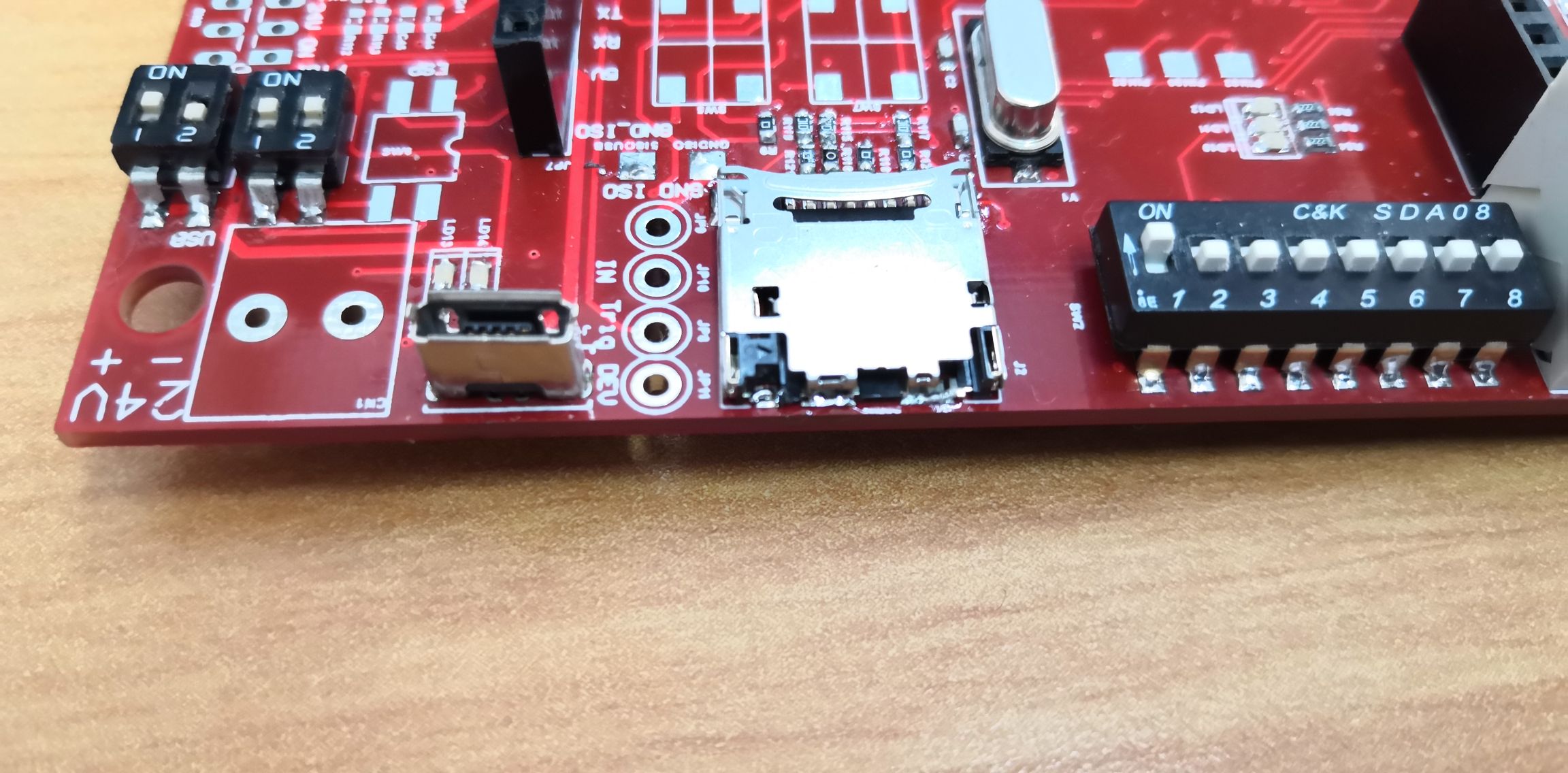
Categories
Recommended Article:
- Quick Turn PCB Manufacturer: Your Reliable Partner for Urgent Projects -NextPCB
- Prevent PCB Insulation Failure: PP Thickness & Stackup Guide
- Best 6-Layer PCB Stackups for Signal Integrity & Impedance Control
- SMT Red Glue: Why It’s Used & How to Optimize for Cost-Effective PCB Assembly
- How to Select the Optimal PCB Hole Size for Through-Hole Pins (Avoid Assembly Failures!)
- Get Early Access to Raspberry Pi RP2354 MCU with NextPCB - NextPCB Accelerator #11
- How to Achieve 50 Ohm Impedance Requirements for PCB Routing without extra charges
- HQDFM PCB Design Analysis Tool User Manual
- Fast Turn Low Volume PCB Assembly Services from China: Speed, Quality & Cost-Efficiency
- NextPCB Lands on Crowd Supply: Supercharging Hardware Startups from Prototype to Production
