

 Printed Circuit Boards
 Surface
 PCB Assembly
 Layer Buildup
 Online Tools
 PCB Design-Aid & Layout
 Mechanics
 SMD-Stencils
 Quality
 Drills & Throughplating
 Factory & Certificate


- PCB Assembly<\/a> Price Including:\r\n\r\n\t<ul>\r\n\t\t<li>Setup fee: $8.00Stencil: $1.50SMT Assembly: $0.0017 per jointHand-soldering labor fee: $3.5\r\n\t\t<p>Manual Assembly: $0.0173 per joint<\/p>\r\n\t\t<\/li>\r\n\t\t<li>Components cost: Based on the components you choose for assembly<\/li>\r\n\t<\/ul>\r\n\t<\/li>\r\n<\/ul>\r\n\r\n<h2>SMT Assembly FAQs<\/h2>\r\n\r\n<p><strong>What does your quoted price include?<\/strong><\/p>\r\n\r\n<p><u>The pcb assembly price includes:<\/u><\/p>\r\n\r\n<ul style=\"margin-left: 40px;\">\r\n\t<li>$8.00<\/li>\r\n\t<li>Stencil: $1.50<\/li>\r\n\t<li>SMT Assembly: $0.0017 per joint<\/li>\r\n\t<li>Hand-Soldering labor fee: $3.5<\/li>\r\n\t<li>Manual Assembly: $0.0173 per joint<\/li>\r\n\t<li>Component Cost: Based on the components you choose for assembly<\/li>\r\n<\/ul>\r\n\r\n<p>Our online quotes will show the exact assembly fee and component cost after you select the parts for assembly<\/p>\r\n\r\n<h2>NextPCB: Custom SMT PCB and Assembly Manufacturer<\/h2>\r\n\r\n<p>Fixing SMD components during <strong>smt pcb assembly<\/strong>requires engineering knowledge and practical skills. Moreover, the chips are extremely sensitive to overheating and come with small outputs. Therefore, fastening with an ordinary soldering iron often leads to their destruction. Without special equipment, mass production is difficult to establish.<\/p>\r\n\r\n<p>By contacting Nextpcb, you can order the manufacture of SMD microcircuits with a guaranteed result. We produce boards in strict accordance with the technical specifications, check the performance of the product with sensitive testers, and fulfill orders, individually approaching each client.<\/p>\r\n\r\n<h2>Conclusion<\/h2>\r\n\r\n<p>In recent years, <strong>smt pcb assembly<\/strong> has become the mainstream for board mounting due to the progress in miniaturization and high density of boards. When using both the SMT process and the IMT process for some products, the SMT process is usually completed first before entering the IMT stage.<\/p>\r\n\r\n<p>Due to market demands and increasing labor costs, IMT is about to replace by SMT. The SMT process is mostly common in fields that require portability, such as mobile phones, PDAs, and GPS. For some products that use high voltage and large current, the percentage of SMD adoption is low due to special parts.<\/p>\r\n","status":1,"create_time":1663640443,"update_time":1686904416,"clicks":12726,"hits":0,"custom_url":"ultimate-guide-to-smt-pcb-assembly","related":"","add_uid":111,"publish_uid":0,"attr":0,"type":0,"keywords":"SMT,Surface Mount Technology, SMT PCB","comment_count":0,"share_count":0,"need_move":0,"c_time":"2022-09-20 10:20:43","u_time":"2025-06-27 15:18:54","comments_count":0,"is_like":0}">

-
- FR-4 is a standard material used as a PCB core. The huge demand for FR-4 material makes it the most affordable material and reduces the delivery time of FR-4 PCBs. The glass transition temperature of FR-4 material is as high as 180C, which might make it an undesirable material for high-temperature applications, but this material has the property to extinguish the fire on itself.<\/p>\r\n\r\n<h3>Metal-Core or Metal-Backed PCB Material<\/h3>\r\n\r\n<p>Metal core PCBs use metals such as Copper and Aluminum as the base material. The PCBs that require high-glass transition temperature, extra mechanical strength and higher dissipation rate should use Metal core to meet their requirements. <\/p>\r\n\r\n<h3>Ceramics<\/h3>\r\n\r\n<p>Ceramic PCBs use aluminum nitride and beryllium oxide as the base material, which provides high thermal conductivity, minimal coefficient of thermal expansion (CTE), and stable dielectric constant (DK), which help in minimizing signal loss.<\/p>\r\n\r\n<h3>High-Frequency Laminates<\/h3>\r\n\r\n<p>High-Frequency Laminates are excellent for circuits that need a faster signal transmission, controlled impedance, low signal loss and least dielectric constant (DK) and dissipation factor (DF). Hence, high-frequency laminates are exceptional for circuits with special requirements and critical applications.<\/p>\r\n\r\n<h2>What Determines the Price of a 10-layer PCB?<\/h2>\r\n\r\n<p>The production cost of the PCB depends on its design, the PCBs with complex designs and non-standard techniques cost more than standard PCBs. We are enlisting five factors that have a high impact on the cost of a 10-layer PCB<\/p>\r\n\r\n<ul style=\"margin-left: 40px;\">\r\n\t<li>Quality of the material and Size of the board<\/li>\r\n\t<li>The thickness of the board<\/li>\r\n\t<li>Temperature resistance property<\/li>\r\n\t<li>Hole dimensions and their quantity on the board<\/li>\r\n\t<li>Other Special requirements<\/li>\r\n<\/ul>\r\n\r\n<p>The standard PCBs use FR-4 as a base material. But PCBs designed for high-tech devices that operate high-frequency, high-speed signals or require high-temperature resistance need high-quality materials such as Rogers and PTEF. High-quality materials are higher in price, and with the large dimensions of boards, the amount of material and fabricating time increased, which impacts the PCB cost.<\/p>\r\n\r\n<p>The extra thin holes require special machinery and skills to drill. Other unique features in a board, such as the thickness of prepreg and solder mask and edge plating, contribute to the price determination of the PCB.<\/p>\r\n\r\n<h2>What Components are Used in a Typical 10-Layer PCB?<\/h2>\r\n\r\n<p>A 10-layer PCB can use all components; some of them are as follow<\/p>\r\n\r\n<ul style=\"margin-left: 40px;\">\r\n\t<li>Resistors<\/li>\r\n\t<li>Diodes<\/li>\r\n\t<li>Capacitors<\/li>\r\n\t<li>Transistors<\/li>\r\n\t<li>Sensors<\/li>\r\n\t<li>LEDs<\/li>\r\n\t<li>Integrated Circuits<\/li>\r\n\t<li>Transformers<\/li>\r\n\t<li>Voltage Regulators<\/li>\r\n\t<li>Connectors<\/li>\r\n\t<li>Fuses<\/li>\r\n<\/ul>\r\n\r\n<h2>How to Arrange the Signal, Power, and Ground Planes on a 10-Layer PCB Stack-up?<\/h2>\r\n\r\n<p>Because a 10-layer PCB has more layers than 2-layer and 4-layer PCB, the arrangement of layers and planes is easy, as there is no shortage of space. What we need to focus on are the fundamental rules of PCB designing.<\/p>\r\n\r\n<p>There is plenty of space to route signal traces, but routing is not the only goal to achieve, but what is crucial is to maintain the signal and power integrity.<\/p>\r\n\r\n<p>Whenever deciding on the arrangement of the signal, power and ground layers focus on these things.<\/p>\r\n\r\n<p>The faster the signal, the higher electromagnetic interference it can create if it does not have a direct current return path. In this situation, having a plane adjacent to signal layers is beneficial as it provides direct return paths and shields the layers against cross talk.<\/p>\r\n\r\n<p>To reduce volt drop in a 10-layer PCB, try to have at least one power plane that is best if adjacent to the layer with the highest-frequency signals.<\/p>\r\n\r\n<p>If the PCB has to operate under a high electromagnetic environment, consider dedicating the top and bottom layers as a ground plane to shield the circuit from external electromagnetic interference.<\/p>\r\n\r\n<p>A considerable stack-up for a low to medium frequency 10-layer PCB is<\/p>\r\n\r\n<ul style=\"margin-left: 40px;\">\r\n\t<li>Signal<\/li>\r\n\t<li>Ground<\/li>\r\n\t<li>Signal<\/li>\r\n\t<li>Power<\/li>\r\n\t<li>Signal<\/li>\r\n\t<li>Ground<\/li>\r\n\t<li>Ground<\/li>\r\n\t<li>Signal<\/li>\r\n\t<li>Power<\/li>\r\n\t<li>Signal<\/li>\r\n<\/ul>\r\n\r\n<h2>Factors that Determine the Designs of a 10-layer PCB Stack-up<\/h2>\r\n\r\n<p>The design of a PCB (including stack-up and layout design) depends on several factors; it gets changed with the requirements and operating conditions of the PCB. Some of the main factors that influence the overall design of the PCB are<\/p>\r\n\r\n<ul style=\"margin-left: 40px;\">\r\n\t<li>Area of application<\/li>\r\n\t<li>Design configurations<\/li>\r\n\t<li>Electrical specifications<\/li>\r\n\t<li>Cost of designing and production<\/li>\r\n\t<li>Component density<\/li>\r\n<\/ul>\r\n\r\n<h3>Area of Application<\/h3>\r\n\r\n<p>The area of application is the main factor that determines the design of the PCB because each domain has specific requirements. For example, high-frequency circuits require extra shielding, whereas PCBs that operate under an electromagnetic environment require higher electromagnetic compatibility. These differences in their working domains define their characteristics, which are crucial to follow during the designing stage of the PCB to get an accurately functioning PCB. <\/p>\r\n\r\n<h3>Design Configurations<\/h3>\r\n\r\n<p>The PCB is a part of a module. If the module has specific conditions for the PCB, its design should follow those conditions. For example, if the module lacks space and can not fit a rigid PCB. The designers can find a substitute for rigid PCBs in flexible PCBs, which are proven more reliable against continuous mechanical pressure and vibration. Other hardware configurations also affect the PCB design in various terms, but the designers can tackle these obstacles by modifying the design and following the best PCB designing practices.<\/p>\r\n\r\n<h3>Electrical Specifications<\/h3>\r\n\r\n<p>electrical specifications of the board, such as signal integrity, electromagnetic compatibility and heat dissipation requirements of the circuit, also affect the design of the PCB in terms of the quality and thickness of material and routing style.<\/p>\r\n\r\n<h3>Cost of Designing and Production<\/h3>\r\n\r\n<p>The PCBs with specific electrical requirements usually demand unusual time and machinery at the fabrication stage. The designers also charge extra for integrating special features. To manage the manufacturing cost of the PCB, the designers try to keep the PCB design as near to the standard design as possible.<\/p>\r\n\r\n<h3>Component Density<\/h3>\r\n\r\n<p>Component density plays a significant role in deciding the layers of the PCB. The higher the components, the larger space required to manage their leads and route them. In this case, having multiple layers to route signals prevents parallel, long traces.<\/p>\r\n\r\n<h2>Layout and Designing Tips for an 8-Layer PCB<\/h2>\r\n\r\n<ul style=\"margin-left: 40px;\">\r\n\t<li>A 10-layer PCB is considerable for routing high-speed signals. But long parallel signals with higher transmission speeds can generate electromagnetic interference. To minimize EMI issues and cross-talk, try to keep such traces on a layer adjacent to the ground plane. <\/li>\r\n\t<li>If the 10-layer PCB is utilizing several voltages, consider splitting the Power plane.<\/li>\r\n\t<li>To eliminate cross-talk and noise route signals perpendicular on each layer and increase the width between the traces, especially increase space between power traces to ensure power integrity.<\/li>\r\n\t<li>If the 10-layer PCB is utilizing both through-hole and surface mounting methods, do consider keeping the temperature resistance properties accordingly.<\/li>\r\n\t<li>The 10-layer PCB is dense in layers. Hence, it generates more heat. Place vias near heat-generating sources; it will boost heat dissipation.<\/li>\r\n\t<li>When designing a 10-layer PCB, check for the component availability before designing the layout, as some components are not-accessible or the manufacturers no longer produce them. In this case, you have to find alternatives that may vary in packaging size and shape. To avoid placement and size issues, check for the availability of components in the market.<\/li>\r\n<\/ul>\r\n\r\n<h2>What is the Difference Between 4-layer and 10-Layer PCB?<\/h2>\r\n\r\n<h3>Performance<\/h3>\r\n\r\n<p>There is an enormous difference in the layers of a 4-layer and a 10-layer PCB. Hence, in the performance and cost. A 10-layer PCB provides many opportunities to divide the structure between signal layers and planes. This feature of a 10-layer PCB improves its performance as power and ground planes provide shielding, return path for current and reduce volt drop. If concerning electromagnetic compatibility, a 10-layer PCB is more reliable than a 4-layer PCB.<\/p>\r\n\r\n<h3>Cost<\/h3>\r\n\r\n<p>The cost of a 10-layer PCB is more than double that of a 4-layer PCB.<\/p>\r\n\r\n<h3>Pros of using a 10-Layer PCB Over a 4-Layer PCB<\/h3>\r\n\r\n<ul style=\"margin-left: 40px;\">\r\n\t<li>More space for signal traces <\/li>\r\n\t<li>higher shielding due to individual power and ground planes<\/li>\r\n\t<li>Excellent current handling capability<\/li>\r\n\t<li>Stronger anti-interference property<\/li>\r\n<\/ul>\r\n\r\n<h3>Cons of using a 10-Layer PCB Over a 4-Layer PCB<\/h3>\r\n\r\n<p>A significant downside of using a 10-layer PCB over a 4-layer PCB is its high design and manufacturing cost.<\/p>\r\n\r\n<h3>Pros of a 10-Layer PCB<\/h3>\r\n\r\n<p>There are numerous advantages of a 10-layer PCB; they include <\/p>\r\n\r\n<ul style=\"margin-left: 40px;\">\r\n\t<li>Higher density for components<\/li>\r\n\t<li>Reliable performance for high-speed and high-frequency circuits.<\/li>\r\n\t<li>Increased power integrity and better options for current return paths.<\/li>\r\n\t<li>The 10-layer PCBs provide robust performance against thermal and mechanical pressure.<\/li>\r\n<\/ul>\r\n\r\n<h3>Cons of a 10-Layer PCB<\/h3>\r\n\r\n<ul style=\"margin-left: 40px;\">\r\n\t<li>A 10-layer PCB has a complex design. Due to this, it requires more time and special machinery for fabricating. These requirements of a 10-layer PCB leads to higher manufacturing cost with potential delay in the delivery time.<\/li>\r\n\t<li>10-layer PCBs are hard to troubleshoot and modify once they are stacked. Hence, they require a keen understanding of PCB design and manufacturing.<\/li>\r\n<\/ul>\r\n\r\n<h2>Applications of a 10-Layer PCB Stack-up<\/h2>\r\n\r\n<p>10-layer PCBs have applications in most sensitive devices and machines, including military and aerospace devices. A list of application areas of 10-layer PCB is as under<\/p>\r\n\r\n<ul style=\"margin-left: 40px;\">\r\n\t<li>Medical equipment<\/li>\r\n\t<li>Smartwatches and home appliances<\/li>\r\n\t<li>Computer and mobiles<\/li>\r\n\t<li>Industrial heavy machinery<\/li>\r\n\t<li>Telecommunication<\/li>\r\n\t<li>Satellites <\/li>\r\n\t<li>power amplifiers<\/li>\r\n\t<li>Automotive industry<\/li>\r\n\t<li>Military and defence<\/li>\r\n<\/ul>\r\n\r\n<h2>What is the Manufacturing Process of a 10-Layer PCB Stack up?<\/h2>\r\n\r\n<p>The manufacturing process of a 10-layer PCB starts from the testing of the layout file and has several stages after it,<\/p>\r\n\r\n<p style=\"margin-left: 40px;\">1. As we stated, the first stage is to check the layout file and approve it for further process.<\/p>\r\n\r\n<p style=\"margin-left: 40px;\">2. The approved files then go for the printing of photo tools, which is a process of converting copper traces onto films by using a plotter.<\/p>\r\n\r\n<p style=\"margin-left: 40px;\">3. Then the photo tools are converted onto the laminates, which are thick sheets of base material coated with copper. <\/p>\r\n\r\n<p style=\"margin-left: 40px;\">4. Then these PCB laminates undergo pressure wash, which uses a strongly alkaline material to etch excess copper from the laminates.<\/p>\r\n\r\n<p style=\"margin-left: 40px;\">5. After the pressure wash, the laminates go for automatic optical inspection to identify errors. At this stage, identifying errors is essential as it is impossible to modify the laminates once they are stacked. <\/p>\r\n\r\n<p style=\"margin-left: 40px;\">6. The next step is to punch registration holes which helps in aligning all the laminates, prepreg and copper sheets together on the binding stage.<\/p>\r\n\r\n<p style=\"margin-left: 40px;\">7. Now, on a base of steel, all the laminates, prepreg sheets, and top and bottom copper layers are stacked one by one and aligned using previously punched holes. <\/p>\r\n\r\n<p style=\"margin-left: 40px;\">8. Once everything is stacked and aligned, the manufacturer placed the top part of the steel plate and screwed the top and bottom steel plates together. <\/p>\r\n\r\n<p style=\"margin-left: 40px;\">9. Then this stack-up undergoes a specific pressure and heat. The heat melts the prepreg, and pressure helps to bind all the laminates and copper layers.<\/p>\r\n\r\n<p style=\"margin-left: 40px;\">10. After the binding of the layers, the manufacturer prints and prepares the top and bottom layers by following the same process as the inner layers.<\/p>\r\n\r\n<p style=\"margin-left: 40px;\">11. Then the stack-up needs to drill holes and vias that need to deposit with some conducting material as the prepreg and laminates are non-conductive.<\/p>\r\n\r\n<p style=\"margin-left: 40px;\">12. Once the electroplating is done, the PCB is ready for a coat of solder mask and then silk screening to print the required information on the outer layers of the PCB.<\/p>\r\n\r\n<p style=\"margin-left: 40px;\">13. The last stage of PCB manufacturing is to test the PCB against the layout file and deliver it to its owner if there are no issues.<\/p>\r\n\r\n<h2>10-Layer PCB Manufacturer - Nextpcb<\/h2>\r\n\r\n<p>NextPCB has been providing high-quality tested 10-layer PCBs for more than 15 years. We are manufacturing a wide range of 10-layer PCBs with different base materials and special manufacturing requirements. Quality is the foremost priority of NextPCB. Hence, we perform several tests on our manufactured 10-layer PCBs to ensure the delivery of a flawless PCB. The NextPCB provides all the stack-ups mentioned above. But if you need a custom-made multilayer PCB with unique specifications and a particular manufacturing process, contact us to get a quick quote within 24 hours.<\/p>\r\n\r\n<h2> Conclusion<\/h2>\r\n\r\n<p>A 10-layer PCB is a high-performance and durable electronic circuit board with several prominent features. A characteristic of a 10-layer PCB is that it provides numerous stack-up options that help to cover a wide range of special requirements. The price of a 10-layer PCB depends on several factors, such as the thickness of the PCB, type of material and manufacturing process. A 10-layer PCB provides good electromagnetic compatibility and reduces EMI issues. But, for high-frequency boards, a 10-layer PCB with standard FR-4 material is not compatible enough. But, with high-quality base materials like Rogers and PTEF, a 10-layer PCB can be excellent for several sensitive and high-performance demanding industries, such as military, aerospace and telecommunication.<\/p>\r\n","status":1,"create_time":1663321406,"update_time":1665457582,"clicks":3804,"hits":2,"custom_url":"high-quality-10-layer-pcb-fabrication","related":"","add_uid":111,"publish_uid":0,"attr":0,"type":0,"keywords":"10 layer pcb,10 layer pcb fabrication","comment_count":0,"share_count":0,"need_move":0,"c_time":"2022-09-16 17:43:26","u_time":"2025-06-27 16:17:07","comments_count":0,"is_like":0}">
- PCB assembly<\/a>, quality testing, and the final shipment. Briefly, NextPCB can meet all your PCB requirements, from PCB prototyping to small or mass PCB production.<\/p>\r\n\r\n<p>>>Get a quick <a href=https://www.nextpcb.com/"https:////www.nextpcb.com//pcb-quote/">online PCB quote<\/a> within 24 hours<<<\/p>\r\n\r\n<h2>Conclusion<\/h2>\r\n\r\n<p>A 12-layer PCB stack-up provides twelve conducting layers to route signal traces. These twelve layers divide into signal layers, Ground and Power planes. The average number of planes that we can have in a 12-layer PCB is 5-6; the rest of the layers are dedicated to routing the signal traces.<br \/>\r\nThe higher number of Ground and Power planes in a 12-layer PCB provides maximum isolation among the signal layers, eliminates cross-talk, and reduces electromagnetic interference (EMI) issues.<\/p>\r\n\r\n<p>A 12-layer PCB provides electromagnetic compatibility and interplane capacitance, which eliminates internal and external electromagnetic interference among the signals. This feature of a 12-layer PCB ensures signal integrity and maximum shielding and provides better opportunities to route high-frequency, high-speed and mixed signals. <\/p>\r\n\r\n<p>The 12-layer PCBs have numerous features, but these features alone are not enough to fulfil the requirements of every individual PCB. The performance of a 12-layer PCB depends on its stack-up design. Even very little negligence at the stack-up designing level can cause issues later. The stack-ups designed by considering several aspects always perform well. Thus, the designers should try their best to understand the requirements of a circuit to construct an equally functional stack-up. <\/p>\r\n\r\n<p>Due to their mechanical strength and durability, the 12-layer PCBs have several applications, especially under harsh environmental conditions.<\/p>\r\n","status":1,"create_time":1663298887,"update_time":1687766391,"clicks":8008,"hits":6,"custom_url":"12-layer-pcb-stackup","related":"","add_uid":111,"publish_uid":0,"attr":0,"type":0,"keywords":"12 layer pcb,12 layer pcb stackup","comment_count":0,"share_count":0,"need_move":0,"c_time":"2022-09-16 11:28:07","u_time":"2025-06-27 15:38:54","comments_count":0,"is_like":0}">
-
- PCB manufacturers<\/a> understand the importance of maintaining PCB quality at all stages of manufacturing. Most manufacturers follow <a href=https://www.nextpcb.com/"https:////www.nextpcb.com//blog//ipc-standard-to-pcb-layout-design/">IPC design layout standards<\/a> and IPC manufacturing. These standards help them maintain PCB quality during the design, test, and inspection phases.<\/p>\r\n\r\n<h2>A Brief Understanding of IPC<\/h2>\r\n\r\n<p>IPC is a trade organization that standardizes requirements for the PCB production and <a href=https://www.nextpcb.com/"https:////www.nextpcb.com//pcb-assembly-services/">PCB assembly<\/a>. The organization was founded in 1957 as the Printed Circuit Board Institute and the Institute for the Interconnection and Packaging of Electronic Circuits. Since 1999, the organization is now officially known as the IPC, which publishes standards for acceptability in the printed circuit board industry. These standards have been accepted worldwide. Currently, IPC has more than 4800 members. These members include companies that specialize in all aspects of PCB manufacturing, from designers to material suppliers to board manufacturers, assembly services and OEMs.<\/p>\r\n\r\n<h2>Understanding the IPC Performance Classes<\/h2>\r\n\r\n<h3>Performance Classes<\/h3>\r\n\r\n<p>Three general classes have been established to reflect progressive increases in sophistication, functional performance requirements and testing\/inspection frequency. It should be recognized that there may be an overlap of equipment categories in different classes. The user has the responsibility to specify in the contract or purchase order, the performance class required for each product and shall indicate any exceptions to specific parameters, where appropriate.<\/p>\r\n\r\n<h4>IPC Class 1:<\/h4>\r\n\r\n<p>General Electronic Products — Includes consumer products and some computer and computer peripherals suitable for applications where cosmetic imperfections are not important and the major requirement is function of the completed printed board.<\/p>\r\n\r\n<h3>IPC Class 2:<\/h3>\r\n\r\n<p>Dedicated Service Electronic Products — Includes communications equipment, sophisticated business machines, instruments where high performance and extended life are required and for which uninterrupted service is desired but not critical. Certain cosmetic imperfections are allowed.<\/p>\r\n\r\n<h3>IPC Class 3:<\/h3>\r\n\r\n<p>High Reliability or Harsh Operating Environment Electronic Products — Includes the equipment and products where continued performance or performance on demand is critical. Equipment downtime cannot be tolerated and must function when required such as in life support items or flight control systems. Printed boards in this class are suitable for applications where high levels of assurance are required and service is essential.<\/p>\r\n\r\n<p><strong>Please NOTE that the final performance class for printed board assemblies (assembled, soldered, cleaned and tested) cannot be any greater than the performance class called out for the bare printed board.<\/strong><\/p>\r\n\r\n<p><strong>That is, in order to obtain a Class 3 with the assembly printed board assembly, an IPC Class 3 recognition of the bare printed board (anything with a Class 2 or 1 with the bare printed board prevents obtaining a Class 3 with the printed board assembly) must be first obtained.<\/strong><\/p>\r\n\r\n<h2>Important IPC Standard for PCB Manufacturing<\/h2>\r\n\r\n<p>Design rules differ between these IPC performance classes, so manufacturers must take them into account when undertaking projects that fit into any of these classes. IPC6012 and IPC-A-600 are two important IPC standards for PCB manufacturing that cover PCB inspection and performance. Each PCB manufacturer must refer to or comply with them during the PCB manufacturing and assembly process.<\/p>\r\n\r\n<h3>IPC -A- 600: Acceptability of Printed Boards<\/h3>\r\n\r\n<p>Also known as <a href=https://www.nextpcb.com/"https:////www.ipc.org//TOC//IPC-A-600J.pdf/" rel=\"noopener nofollow\">IPC-600<\/a>, this specification sets the level of acceptance criteria for each product category. The specification outlines the objectives and acceptable and unacceptable conditions for each product. These conditions may be found in internal or external observations. The specification focuses on the visual interpretation of the requirements presented in the various PCB specifications.<\/p>\r\n\r\n<h3>IPC-6012: Performance Requirements for Rigid Printed Circuit Boards<\/h3>\r\n\r\n<p><a href=https://www.nextpcb.com/"https:////www.ipc.org//TOC//IPC-6012D.pdf/" rel=\"noopener nofollow\">IPC-6012<\/a> provides a detailed overview of the performance requirements and qualifications for rigid printed circuit boards. Rigid circuit boards can be designed in a variety of ways, such as single-sided PCBs, active\/passive embedded PCBs, metal core PCBs, HDI, etc. All these designs and their performance requirements are broadly classified in this standard.<\/p>\r\n\r\n<h2>How PCB Manufacturers Benefit from IPC Standards<\/h2>\r\n\r\n<p>Compliance with these standards will help PCB manufacturers benefit in the following ways.<\/p>\r\n\r\n<p>Maintaining quality and consistency: As with any other industry standard, the IPC standards for PCB manufacturing are designed to improve quality for PCB manufacturers. As mentioned earlier, these standards control every stage of manufacturing. As a result, manufacturers who strictly adhere to these requirements can be assured of a quality product. By following the specifications and their requirements, manufacturers can ensure consistent quality, which will ultimately improve customer satisfaction.<\/p>\r\n\r\n<p>Ensure seamless workflow during manufacturing and assembly: When following IPC standards for PCB manufacturing, it is important to follow specific workflows that have been streamlined and documented, which helps ensure a seamless workflow within the team.IPC standards also help ensure better communication between suppliers, vendors, customers, regulatory agencies, etc.<\/p>\r\n\r\n<p>Build brand reputation: Most OEMs know the importance of PCBs and therefore prefer to work with PCB manufacturing and assembly service providers that follow IPC standards for PCB manufacturing. This is because these standards help minimize assembly or manufacturing-related errors and produce a quality product. This helps manufacturers build their brand reputation.<\/p>\r\n\r\n<p>Cost reduction: Needless to say, strict adherence to the PCB manufacturing quality standards set by the IPC standards will help minimize manufacturing errors and material loss, and minimize the need for testing and inspection.<\/p>\r\n","status":1,"create_time":1661935289,"update_time":1661935554,"clicks":3432,"hits":1,"custom_url":"important-ipc-standards-for-pcb-manufacturing","related":"","add_uid":111,"publish_uid":0,"attr":0,"type":0,"keywords":"IPC standard","comment_count":0,"share_count":0,"need_move":0,"c_time":"2022-08-31 16:41:29","u_time":"2025-06-27 15:56:39","comments_count":0,"is_like":0}">
Important IPC Standards for PCB Manufacturing
This article introducts the importance, performance classed of IPC standard for PCB manufacturing.
3432 1 0 Shares
- PCB manufacturers<\/a> understand the importance of maintaining PCB quality at all stages of manufacturing. Most manufacturers follow IPC standards for PCB manufacturing. These standards help them maintain PCB quality during the design, test, and inspection phases. <\/p>\r\n\r\n<p><a href=https://www.nextpcb.com/"http:////www.ipc.org//ipc-history/" rel=\"noopener nofollow\">The Institute for Interconnecting and Packaging Electronic Circuits(IPC)<\/a> is a trade organization that standardizes requirements for the manufacture and assembly of printed circuit boards. The organization was founded in 1957 as the Institute of Printed Circuit and the Institute for the Interconnection and Packaging of Electronic Circuits. Since 1999. Today the organization is now formally known as IPC, which publishes standards for the acceptability of the printed circuit board industry. These standards have been accepted worldwide. Currently, IPC has more than 4800 members. These members include companies that specialize in all aspects of PCB manufacturing, from designers to material suppliers to board manufacturers, assembly services and OEMs.<\/p>\r\n\r\n<h2>IPC Standard Tree<\/h2>\r\n\r\n<p><img alt=\"IPC Standard Tree\" src=https://www.nextpcb.com/"//uploads//images//202208//31//1661929803-2964-uTcqoV.jpg/" style=\"width: 800px; height: 1035px;\" \/><\/p>\r\n\r\n<p>This standards tree shows the classification and specifications needed for manufacturing aspects such as:<\/p>\r\n\r\n<p><strong>Design<\/strong>: The <a href=https://www.nextpcb.com/"http:////www.ipc.org//TOC//IPC-2221A.pdf/" rel=\"noopener nofollow\">IPC-2221<\/a> series are generic standards for the planning of PCBs. This covers everything from board flexibility and rigidity to the planning layout, elements lists, material selections, and a number of other further properties. <\/p>\r\n\r\n<p><strong>Manufacturing<\/strong>: The <a href=https://www.nextpcb.com/"http:////www.ipc.org//TOC//IPC-6012D.pdf/" rel=\"noopener nofollow\">IPC-6012<\/a> provides a detailed overview of the performance requirements and qualifications of rigid printed circuit boards. Rigid circuit boards can be designed in a variety of ways, such as single-sided PCBs, active\/passive embedded PCBs, metal core PCBs, HDI, etc. All these designs and their performance requirements are broadly classified in this standard.<\/p>\r\n\r\n<p><strong>Inspection<\/strong>: The <a href=https://www.nextpcb.com/"http:////www.ipc.org//ipc-600-acceptability-printed-boards-endorsement-program/" rel=\"noopener nofollow\">IPC-A-600<\/a> includes standards for the principles of written boards, like product classification, acceptance criteria, conductor breadth and spacing, stuff material criteria, and more. These standards may be peer-to-peer training-related, testing-related, etc. <\/p>\r\n\r\n<p><strong>Performance<\/strong>: <a href=https://www.nextpcb.com/"http:////shop.ipc.org//6012-0-b-swedish/" rel=\"noopener nofollow\">IPC-6012B<\/a> provides performance needs encompassing the structural integrity, solderability, and area needs for rigid PCBs. <\/p>\r\n\r\n<p><strong>Assembly<\/strong>: <a href=https://www.nextpcb.com/"http:////www.ipc.org//ipc-610-acceptability-electronics-assemblies-endorsement-program/" rel=\"noopener nofollow\">IPC-A-610<\/a> is the "Acceptability of Electronic Assemblies" customary, that outlines specific fastening and mounting criteria. <\/p>\r\n\r\n<p><strong>Cleaning<\/strong>: sure uses of PCBs need the utmost cleanliness. <a href=https://www.nextpcb.com/"https:////www.ipc.org//sites//default//files//test_methods_docs//2-3_2-3-25-1.pdf/" rel=\"noopener nofollow\">IPC-TM-650-2.3.25.1<\/a> covers ways for ionic cleanliness testing for clean boards. <\/p>\r\n\r\n<p><strong>Much more<\/strong><\/p>\r\n\r\n<p>Keep up on recent revisions by sorting out this <a href=https://www.nextpcb.com/"http:////www.ipc.org//ipc-document-revision-table/" rel=\"noopener nofollow\">IPC standards revision list<\/a>.<\/p>\r\n\r\n<p>To get specifics on every standard, use this <a href=https://www.nextpcb.com/"http:////www.ipc.org//media//3418//download/" rel=\"noopener nofollow\">IPC Checklist<\/a>.<\/p>\r\n\r\n<h2>Why Is It Important to Comply With IPC Standards for PCB Layout Design?<\/h2>\r\n\r\n<p>It's tedious to browse through pages of IPC standards, however, they're there permanently reasons, notably for PCB layout styles. The IPC was established in 1957 and at the time was referred to as the Institute of computer circuit. Today the organization is now formally known as IPC, which publishes standards for the acceptability of the printed circuit board industry. These standards have been accepted worldwide. Currently, IPC has more than 4800 members. These members include companies that specialize in all aspects of PCB manufacturing, from designers to material suppliers to board manufacturers, assembly services and OEMs.. <\/p>\r\n\r\n<p>IPC produces and maintains standards that function a typical guideline for PCB style, fabrication, assembly, test, and different areas of concern. For PCB designers, obliging with the relevant IPC standards for PCB layouts will create a distinction during a product's success or failure.<\/p>\r\n\r\n<p>There area unit simply too several variables in PCB style that may have an effect on the dependableness and manufacturability of a board. for instance, designers might intercommunicate estimate for the right pad size for through-hole parts. coming up with while not the steerage of IPC standards may also cause non-conformance of uniformity between designers and makers.<\/p>\r\n\r\n<h2>Which IPC Standard Should You Use for PCB Design Layouts?<\/h2>\r\n\r\n<h3>IPC-2221<\/h3>\r\n\r\n<p>Throughout the times, the IPC has established colorful norms that insure design trustability and manufacturability. For PCB contrivers, the must-have- read IPC standard is the IPC- 2221. The IPC- 2221 is the general standard that covers nearly every aspect of PCB design.<\/p>\r\n\r\n<p>The standard details how electrical considerations similar as PDN machine layouts, captain concurrence, and impedance control should be enforced on a PCB. You 'll also find runners in the standard that concentrate on thermal design considerations for the PCB. The standard explores multiple methods of dissipating heat in PCBs and explains how to apply them in factual designs.<\/p>\r\n\r\n<p>PCB design and manufacturing are thick sides of the same coin. Some sections of the IPC- 2221 helps contrivers insure the PCB is optimized for PCB manufacturing. For illustration, section 9 touches on holes and interconnections, which contain guidance on drill size, land pattern, and captain distance on a PCB.<\/p>\r\n\r\n<h3>IPC-2222<\/h3>\r\n\r\n<p>Meanwhile, the IPC- 2222 is a standard that dives deeper into the conditions for a rigid organic PCB design. This standard goes into detail on factors that enhance the manufacturability of a rigid PCB, including material selection, hole size, interconnects, and mechanical parcels.<\/p>\r\n\r\n<h3>IPC-2223<\/h3>\r\n\r\n<p>The IPC-2221, however, does now no longer cowl suggestions associated with flex PCB layout. If you're operating on one, you'll want to consult the IPC-2223, which solely specializes in flex PCB shape layout. It covers vital layout concerns consisting of pad\/thru placement, bend radius, coverlays, and structural specs for flex PCBs.<\/p>\r\n","status":1,"create_time":1661930120,"update_time":1661935440,"clicks":5479,"hits":1,"custom_url":"ipc-standard-to-pcb-layout-design","related":"","add_uid":111,"publish_uid":0,"attr":0,"type":0,"keywords":"IPC standard","comment_count":0,"share_count":0,"need_move":0,"c_time":"2022-08-31 15:15:20","u_time":"2025-06-27 16:14:33","comments_count":0,"is_like":0}">
- rigid-flexible FR4 PCBs<\/a>. <\/p>\r\n\r\n<p>Flexibility comes from the flexibility of the perimeter. We used thin boards because they are more flexible and more susceptible to heat.<\/p>\r\n\r\n<p>It may bend during soldering to obtain the desired angle.<\/p>\r\n\r\n<h3><strong>Properties and materials of FR4:<\/strong><\/h3>\r\n\r\n<p>The FR4 material is used under the UL94-0 standard for the flammability of plastics. The code 94-0 would be written on all FR-4 plates, which proves that the device is guaranteed to be protected against the spread of fire when burning the material.<\/p>\r\n\r\n<p>Good PCB FR4 with multiple layers of FR4 glued between two thin layers of the laminated copper plate because bromine is used in its production, which is why it is also called a halogen element.<\/p>\r\n\r\n<p><strong>The standard FR4 PCB has a heat resistance of almost 248 ° F to 266 ° F.<\/strong><\/p>\r\n\r\n<h3><strong>Application of FR4 PCBs<\/strong><\/h3>\r\n\r\n<p>Foiled fiberglass FR 4 is used to produce printed circuit boards for a wide range of military pcb, telecommunications, industrial, and instrumentation equipment. The material is the base for printed circuit boards used in consumer electronics and computer equipment.<\/p>\r\n\r\n<h3><strong>The Difference between FR-4 Material and High-Frequency Laminate<\/strong><\/h3>\r\n\r\n<p>The reliability of an electronic device is primarily influenced by the quality and type of components used during its production. Undoubtedly, printed circuits fall into this category. They enable the proper functioning of the electronic system. The selection of the base laminate on which the circuit will be produced is therefore crucial. <\/p>\r\n\r\n<p><strong>Currently, PCB production uses laminates on the following substrates:<\/strong><\/p>\r\n\r\n<ul>\r\n\t<li>glass-epoxy,<\/li>\r\n\t<li>marked with the symbol FR4<\/li>\r\n\t<li>aluminum MCPCB (Metal Core PCB)<\/li>\r\n\t<li>Similarly, Teflon and ceramic<\/li>\r\n<\/ul>\r\n\r\n<p>The choice of the type of laminate depends on the intended use of the device and its operating conditions.<\/p>\r\n\r\n<h3><strong>What is PCB Laminate?<\/strong><\/h3>\r\n\r\n<p>Laminate is defined as a glass-epoxy, aluminum, Teflon, or ceramic substrate covered on one or both sides with a copper foil, having such technical parameters that enable its use in specific devices. We divide laminate parameters into basic,<\/p>\r\n\r\n<ul>\r\n\t<li>Temperature<\/li>\r\n\t<li>moisture absorption<\/li>\r\n\t<li>Electrical Parameters <\/li>\r\n<\/ul>\r\n\r\n<p><br \/>\r\nTypical PCB designs are based on the use of a standard FR4 glass-epoxy laminate, with an operating temperature of typically -50 to +110 ° C, with a glass transition temperature Tg of about 135 ° C. The dielectric constant Dk can range from 3.8 to 4.6 depending on the supplier and the type of material. <\/p>\r\n\r\n<p>With increased requirements for heat resistance high-temperature, FR4 High Tg or FR5 is used. Polyimide is used with the requirements for constant operation at high temperatures or with sudden temperature drops. <\/p>\r\n\r\n<p>In addition, polyimide is used in the production of tiles with increased reliability, for military applications, and when increased electrical strength is needed. For PCBs with very high frequency (bwcz) circuits - above 2 GHz, individual layers of bwcz material are used or the tile is entirely made of bwcz material. <\/p>\r\n\r\n<h3><strong>FR4 Material Sub-Types<\/strong><\/h3>\r\n\r\n<p>FR-4 materials are the most common for the production of single-sided, double-sided, and multilayer printed circuits with increased requirements in terms of mechanical strength. <\/p>\r\n\r\n<p><strong>Depending on the properties and application, FR-4 is divided into the following subclasses:<\/strong><\/p>\r\n\r\n<ul>\r\n\t<li>Standard, with glass transition temperature Tg ~ 130 ° C, with or without ultraviolet blocking. The most widespread and widely used type, and at the same time the cheapest of the FR-4;<\/li>\r\n\t<li>with high glass transition temperature, Tg ~ 170 ° C- 180 ° C, suitable for lead-free tinning and soldering technology;<\/li>\r\n\t<li>halogen-free, suitable for lead-free tinning and soldering technology;<\/li>\r\n\t<li>with the normalized index of CTI ≥ 400, ≥ 600;<\/li>\r\n<\/ul>\r\n\r\n<h3><strong>High-Frequency Laminate<\/strong><\/h3>\r\n\r\n<p>The durability and reliability of electronic devices depend on the quality and type of components used, including printed circuits, which form the basis of a properly functioning electronic system. For this reason, the appropriate selection of the parameters of the base laminate, ensuring the long and reliable operation of the finished product, is very important.<\/p>\r\n\r\n<h3><strong>Laminate parameters<\/strong><\/h3>\r\n\r\n<h4><strong>1. Basic parameters of laminates:<\/strong><\/h4>\r\n\r\n<ul>\r\n\t<li>The thickness of the dielectric and copper foil - determines the mechanical resistance, fit with the housing, current carrying capacity, etc.<\/li>\r\n\t<li>CTI class - responsible for resistance to punctures between paths in a humid environment;<\/li>\r\n\t<li>Non-flammability class (UL) - determines the degree of flammability of a given material.<\/li>\r\n<\/ul>\r\n\r\n<h4><strong>2. Temperature parameters of laminates:<\/strong><\/h4>\r\n\r\n<ul>\r\n\t<li>glass transition temperature (limit): Tg - yield point;<\/li>\r\n\t<li>the temperature of chemical decomposition of laminate: Td - temperature causing a 5% loss in weight of the laminate;<\/li>\r\n\t<li>time to delamination: T260 \/ 288 - time after which delamination appears in the material (for temperatures 260 and 288 ° C);<\/li>\r\n\t<li>the thermal expansion coefficient of the laminate in the XY plane and the direction of the Z axis: CTEZ, XY;<\/li>\r\n\t<li>Maximum operating temperature MOT - safe temperature for continuous operation.<\/li>\r\n<\/ul>\r\n\r\n<h4><strong>3. Absorption of moisture by laminates:<\/strong><\/h4>\r\n\r\n<ul>\r\n\t<li>maximum moisture content in the laminate;<\/li>\r\n\t<li>Resistance to the CAF phenomenon.<\/li>\r\n<\/ul>\r\n\r\n<h4><strong>4. Electrical parameters of laminates:<\/strong><\/h4>\r\n\r\n<ul>\r\n\t<li>dielectric constant Dk;<\/li>\r\n\t<li>loss Df;<\/li>\r\n\t<li>Dielectric breakdown resistance.<\/li>\r\n<\/ul>\r\n\r\n<h3><strong>PCB Boards with an Aluminum Core<\/strong><\/h3>\r\n\r\n<p>The complexity of systems and the degree of packing of their elements on printed circuits is more and more problematic due to the need to ensure proper heat dissipation, generated in high-power semiconductor elements. <\/p>\r\n\r\n<p>The use of a standard, glass-epoxy FR4 laminate in such devices, high-power components adapted to THT assembly, and typical heat sinks, increases the production costs of these devices, their size, and their weight. <\/p>\r\n\r\n<p>Therefore, PCB manufacturers and designers use laminates on an insulated metal substrate IMS (Insulated Metal Substrate), in the form of an aluminum core, referred to as MCPCB (<a href=https://www.nextpcb.com/"https:////www.nextpcb.com//pcb-vocabulary//metal-core-pcbs/">Metal Core Printed Circuit Board<\/a>).<\/p>\r\n\r\n<h4><strong>Aluminum Core Laminates<\/strong><\/h4>\r\n\r\n<p>Laminates with an aluminum core are characterized by high thermal conductivity, described by the TC value (Thermal Conductivity). In the case of a standard IMS laminate, it is at the level of 2 W \/ mK. There are also materials with a TC of 2-5 W \/ mK available on the market. <\/p>\r\n\r\n<p>For comparison, the TC coefficient of a typical FR4 laminate is by an order lower - 0.3 W \/ mK. In addition, laminates with aluminum core have higher mechanical strength (stiffness) with the same material thickness and lower thermal expansion than FR4.<\/p>\r\n\r\n<h4><strong>The use of FR4 and MCPCB laminates<\/strong><\/h4>\r\n\r\n<p>Ordinary FR4 laminate is intended for the assembly of systems operating with frequencies up to 0.5 GHz. However, there are special varieties of FR4 laminate with better frequency parameters.<\/p>\r\n\r\n<p>Laminates designed to work in the microwave range are based on ceramic (eg Rogers RO4003) or Teflon (eg Rogers RO3003) dielectrics. Another advantage of these laminates is the high Tg temperature of 280 ° C compared to the FR4 laminate.<\/p>\r\n\r\n<p>MCPCB circuits are commonly used in high-power devices, such as switching power supplies (converters) and lighting lamps, where the light sources are matrices of high-power LEDs in SMD casings. <\/p>\r\n\r\n<p>LED lamps of this type are commonly used, among others, in lighting, in the automotive industry as external lights for vehicles, and in street light signals. Laminates for these applications are usually covered with a white solder mask, which increases the reflection of light.<\/p>\r\n\r\n<p>The choice of specific production material is dictated by the assumed working conditions and the type of the designed device. There is also an economic factor in the decision-making process. However, it is worth bearing in mind that the use of high-quality materials has a key impact on the reliability and lifetime of the device.<\/p>\r\n\r\n<h3><strong>Unusual applications of laminates<\/strong><\/h3>\r\n\r\n<p>The laminate typically used in the production of PCBs is also used in non-standard applications, including:<\/p>\r\n\r\n<h4><strong>Front plates<\/strong><\/h4>\r\n\r\n<p>An example is measuring systems worn on the head. They are used, among others in medicine, aviation, and various types of simulators; as well as electric instruments, in toys, e.g. electronic dice or educational robots. <\/p>\r\n\r\n<p>Integrated surface-mounted modules directly to another printed circuit; Examples include commonly used Wi-Fi, Bluetooth or GSM, and GPS modems.<\/p>\r\n\r\n<h4><strong>Adapters for integrated circuits<\/strong><\/h4>\r\n\r\n<p>They allow you to mount elements with a different pin layout or housing on the PCB, without the need to design a newer version of the circuit.<\/p>\r\n\r\n<h4><strong>Planar transformers<\/strong><\/h4>\r\n\r\n<p>Unlike a typical transformer, the windings are made on a copper layer in the form of flat coils. Inside them, holes are made through which the halves of the ferrite core pass. <\/p>\r\n\r\n<p>These types of structures are characterized by: compact structure, small dimensions, no need to use a separate transformer outside the printed circuit (lower cost), low leakage induction, and higher energy efficiency compared to a standard transformer in the form of a separate element.<\/p>\r\n\r\n<h3><strong>Why should pcb manufacturers have adequate knowledge of laminates?<\/strong><\/h3>\r\n\r\n<p>Knowledge of the most important parameters of laminates will allow pcb manufacturers to choose the most optimal laminate tailored to the requirements and operating conditions of a given device. <\/p>\r\n\r\n<p>To ensure a long and trouble-free operation of devices, it is essential to use high-quality laminates. This is often associated with the necessity to incur higher costs. In the long run, however, it is more cost-effective than servicing and repairing devices damaged due to the use of an unsuitable laminate.<\/p>\r\n\r\n<h3><strong>What are FR4 Alternative PCB Materials?<\/strong><\/h3>\r\n\r\n<h4><strong>Paper Phenol Substrate (FR-1, 2)<\/strong><\/h4>\r\n\r\n<p>Mainly used for single-sided substrates. Among the materials, it has been used for a wide range of purposes such as white goods, pre-high-definition TVs, stationary VTRs, stereos, radio cassette recorders, home phones, game consoles, keyboards, and electronic components. ..<\/p>\r\n\r\n<p>Normally, through-holes cannot be formed by plating, but they are used for silver through-hole substrates that form through-holes by filling holes with silver paste and are used for remote controls for game consoles, TVs, and air conditioners, and audio.<\/p>\r\n\r\n<h4><strong>Paper Epoxy Substrate (FR-3)<\/strong><\/h4>\r\n\r\n<p>Used for single-sided boards like paper phenolic boards, but because of their excellent arc resistance, tracking resistance, and moisture resistance, it is used for high-voltage circuits and circuits that require moisture resistance. It seems that there are many cases.<\/p>\r\n\r\n<h4><strong>Glass composite substrate (CEM-3)<\/strong><\/h4>\r\n\r\n<p>Epoxy resin is impregnated into a mat-like material made by cutting and aligning glass fibers. In particular, it has excellent tracking resistance and is cheaper than glass epoxy.<\/p>\r\n\r\n<p>Therefore, it is used in a wide range of double-sided plates, from home appliances and AV equipment related to amusement to some industrial equipment, which cannot be handled by single-sided plates.<\/p>\r\n\r\n<h4><strong>ITEQ IT-180A<\/strong><\/h4>\r\n\r\n<p>Fiberglass IT-180A has a high glass transition temperature Tg (175°C), high thermal stability, low Z-axis CTE, and high reliability. It is compatible with lead-free soldering.<\/p>\r\n\r\n<h4><strong>MI 1222<\/strong><\/h4>\r\n\r\n<p>MI 1222 is a layered pressed material based on fiberglass impregnated with an epoxy binder, lined on one or both sides with electrolytic copper foil.<\/p>\r\n\r\n<ul>\r\n\t<li>surface electrical resistance (Ohm): 7 x 10¹¹;<\/li>\r\n\t<li>specific volume electrical resistance (Ohm m): 1 x 10¹²;<\/li>\r\n\t<li>dielectric constant: 4.8;<\/li>\r\n\t<li>foil peel strength (N): 1.8.<\/li>\r\n<\/ul>\r\n\r\n<h4><strong>FAF-4D<\/strong><\/h4>\r\n\r\n<p>Fiberglass-reinforced PTFE is lined on both sides with copper foil. It is used as the basis of printed circuit boards operating in the microwave range, and as electrical insulation for printed elements of receiving and transmitting equipment. It can work for a long time in the temperature range from -60 to +250 ° C.<\/p>\r\n\r\n<ul>\r\n\t<li>The adhesion strength of the foil to the base per strip is 10 mm, N (kgf), not less than 17.6(1.8);<\/li>\r\n\t<li>Tangent of the dielectric loss angle at a frequency of 106 Hz, no more than 7 x 10 -4 ;<\/li>\r\n\t<li>Dielectric constant at a frequency of 1 MHz: 2.5 ± 0.1;<\/li>\r\n\t<li>Let out sizes of sheets (maximum deviation on width and length of a sheet of 10 mm.) 500 x 500 mm.<\/li>\r\n<\/ul>\r\n\r\n<h3><strong>Tips to Select the Right FR4 Material for Your FR4 PCB<\/strong><\/h3>\r\n\r\n<p>Choosing a printed circuit board material is an important part of the printed circuit board manufacturing process. When designing a printed circuit board, if you know the discrimination of materials, you can choose the printed circuit board suitable for the product, which is useful.<\/p>\r\n\r\n<ul>\r\n\t<li>The material of the general printed circuit board was a combination of resin, reinforcing material (almost glass fiber), and metal copper foil.<\/li>\r\n\t<li>The material properties of the printed circuit board were influenced by the resin content and type. Therefore, it is necessary to select the appropriate printed circuit board material according to various printed circuit board designs.<\/li>\r\n<\/ul>\r\n\r\n<p>Currently, the printed circuit board material often used in the printed circuit board industry is glass epoxy board (FR-4), which is one of the flame-retardant materials.<\/p>\r\n\r\n<h4><strong>Know Your Requirements to Use FR4 Material<\/strong><\/h4>\r\n\r\n<p>First, you need to find out where to use the materials you need and what properties you want the board to have so that you can choose the materials you need.<\/p>\r\n\r\n<p>FR4 chips are typically used for common electronic products. It is the grade of the material, not the name of the material. This means that the resin material must be able to burn itself.<\/p>\r\n\r\n<p>Currently, there are many fr-4 materials used in ordinary circuit boards, but most of them are made of terra-functional epoxy resin, fillers, and heat-resistant fiberglass composites.<\/p>\r\n\r\n<p>Also, when heated, the board bends, the expansion and contraction of the board affect the parts, the electrodes come off, and reliability decreases.<\/p>\r\n\r\n<p>Therefore, it is necessary to select a steel plate with a small curvature, and the FR4 substrate is suitable.<\/p>\r\n\r\n<h4><strong>The following factors should be considered when choosing a PCB board material:<\/strong><\/h4>\r\n\r\n<p>(1) Select an appropriate board with a glass transition temperature (Tg) that is higher than the operating temperature of the circuit.<\/p>\r\n\r\n<p>(2) High heat resistance generally required 50 seconds, 250 ° C \/ heat resistance.<\/p>\r\n\r\n<p>(3) Good flatness. SMT requires the use of boards with the smallest possible curvature and warpage of less than 0.0075 mm \/ mm.<\/p>\r\n\r\n<p>(4) The coefficient of thermal expansion is low. Since the coefficients of thermal expansion of X and Y do not match the thickness direction, the PCB is prone to deformation. In severe cases, the metalized holes will break and cause component damage.<\/p>\r\n\r\n<p>(5) Electrical performance. For high-frequency circuits, it is necessary to select a material with a high dielectric constant and low dielectric loss. Insulation resistance, voltage strength, and arc resistance must meet product requirements. Knowing some of the board selection factors above, the author believes that choosing a board material can save a lot of effort<\/p>\r\n\r\n<h3><strong>Factors to Consider When Choosing the Thickness<\/strong><\/h3>\r\n\r\n<h4><strong>1. Sheet thickness:<\/strong><\/h4>\r\n\r\n<p>The thickness depends on the project you want to build. The thinnest boards are widely used for the printed circuit boards they're designed for.<\/p>\r\n\r\n<p>Thin PCBs reduce stress. Ideally, you'd need an FR4 thickness of nearly 1-3 inches.<\/p>\r\n\r\n<h4><strong>2. Impedance Matching<\/strong><\/h4>\r\n\r\n<p>In electrical and electronic equipment, impedance or frequency matching is very important for low or high-frequency printed circuit boards.<\/p>\r\n\r\n<p>Paying more attention to these points will help your board get up and running safely. It can also tell you about the capacitance of a multifaceted board.<\/p>\r\n\r\n<h4><strong>3. Flexibility<\/strong><\/h4>\r\n\r\n<p>Thin boards are more flexible than thick boards. Most manufacturers use thin boards compared to thick boards because of their flexibility.<\/p>\r\n\r\n<p>While using FR4, if the board you are using is very thin and your FR4 PCB has more area or dimensions, you will be at great risk.<\/p>\r\n\r\n<p>Thin FR4 PCB with the ability to reduce stress in electrical and electronic devices.<br \/>\r\nThin boards are more flexible and more susceptible to heat.<br \/>\r\nIt can be bent to any desired angle while soldering.<\/p>\r\n\r\n<h4><strong>4 Compatibility with components<\/strong><\/h4>\r\n\r\n<p>FR4 is useful for producing various kinds of printed circuit boards; thickness and spacing are used for devices or components FR4 PCB.<\/p>\r\n\r\n<p>Similar to using the THT method, a thinner PCB design is required because the device is different from other devices.<\/p>\r\n\r\n<h3><strong>How Is FR-4 Used in PCBs?<\/strong><\/h3>\r\n\r\n<p>FR4 is the fundamental part of the printed circuit board which has a comprehensive lamination of the copper foil layers. FR4 pcb board manufacturers apply this lamination with the help of heat and adhesives.<\/p>\r\n\r\n<p>During the FR4 PCB manufacturing process, the FR4 boards are laminated with copper layers at a specific temperature.<\/p>\r\n\r\n<p>It is ideal for insulation as well as board supports without laminated copper and has a higher TG of around 180 ° C.<\/p>\r\n\r\n<h3><strong>When to Avoid FR4 Material?<\/strong><\/h3>\r\n\r\n<p><strong>FR4 material is not the best thing if you want to build a product under the following requirement:<\/strong><\/p>\r\n\r\n<ul>\r\n\t<li>Excellent temperature resistance. FR4 materials are not recommended for highly extreme temperatures.<\/li>\r\n\t<li>High-frequency signals. FR4 material cannot maintain accurate high-frequency signals.<\/li>\r\n\t<li>Lead-free soldering. During reflow soldering, the temperature can catch its peak which can be dangerous for the fr4 material.<\/li>\r\n<\/ul>\r\n\r\n<h3><strong>Nextpcb's Standard FR-4 Material Properties<\/strong><\/h3>\r\n\r\n<ul>\r\n\t<li>Real Value according to the Nextpcb:<\/li>\r\n\t<li>High Glass Transition Temperature (Tg) (150Tg or 170Tg)<\/li>\r\n\t<li>High Decomposition Temperature (Td) (> 345º C)<\/li>\r\n\t<li>Low Coefficient of Thermal Expansion (CTE) ((2.5%-3.8%)<\/li>\r\n\t<li>Dielectric Constant (@1 GHz): 4.25-4.55<\/li>\r\n\t<li>Dissipation Factor (@ 1 GHz): 0.016<\/li>\r\n\t<li>UL rated (94V-0, CTI = 3 minimum)<\/li>\r\n\t<li>Compatible with standard and lead-free assembly.<\/li>\r\n\t<li>Laminate thickness available from 0.005" to 0.125"<\/li>\r\n<\/ul>\r\n\r\n<h3><strong>Conclusion<\/strong><\/h3>\r\n\r\n<p>Thin FR4 material is widely used in applications where space is always limited. These materials are known to provide better flexibility, so they are used to build complex and thin PCBs used in the medical and automotive industries.<\/p>\r\n\r\n<p>Choose a material that has a uniform dielectric constant at different frequencies, FR4 is suitable for this. Avoid using other thin PCB materials with grooves as this may result in a high risk of breaking or damaging the board.<\/p>\r\n\r\n<p>With the same needs, FR4 is manufactured and available in a variety of sizes and configurations. Their favorable physical and chemical properties have contributed to their popularity.<\/p>\r\n\r\n<p>If you plan to consider FR4 in your upcoming electronics application, it is always a good practice to consult with industry players who may provide technical assistance including material selection.<\/p>\r\n\r\n<h3><strong>Why NextPCb for your future FR4 PCB order?<\/strong><\/h3>\r\n\r\n<p>NextPCB delivers full turnkey service and on-time delivery with free shipping globally. Our PCB manufacturing capabilities can accelerate contemporary printed circuit board requirements that include major industries like military, medical, security, automotive, and power.<\/p>\r\n","status":1,"create_time":1661852762,"update_time":1743044916,"clicks":6958,"hits":5,"custom_url":"fr-4-pcb","related":"","add_uid":111,"publish_uid":0,"attr":0,"type":0,"keywords":"FR-4 PCB, FR-4, fr4 pcb, fr4 pcb manufacturer","comment_count":0,"share_count":0,"need_move":0,"c_time":"2022-08-30 17:46:02","u_time":"2025-06-27 16:41:30","comments_count":0,"is_like":0}">
- PCB quote<\/a> page to re-input parameters after Kicad finished the design? We fully understand your feeling, so today we have specially solved this trouble for you.<\/p>\r\n\r\n<p><img alt=\"NextPCB Plugins-In for KiCad\" src=https://www.nextpcb.com/"//uploads//images//202208//19//1660895090-9242-VEuJTi.gif/" style=\"width: 800px; height: 450px;\" \/><br \/>\r\nWhen you click NextPCB Plug-in button on Kicad, we will export these files to your project:<\/p>\r\n\r\n<p>1. Gerber files in the correct format for production<br \/>\r\n2. IPC-Netlist file<br \/>\r\n3. Bom-file that includes all information of components<br \/>\r\n4. Pick and Place-file used in the assembly<\/p>\r\n\r\n<p>You can click "Save to Cart" to place an order immediately after uploading the files(which usually only takes a few seconds), our engineers will double-check the files before production.<\/p>\r\n\r\n<h2><br \/>\r\nHow to Install NextPCB Plugin from Official KiCad Repositories?<\/h2>\r\n\r\n<h3> <\/h3>\r\n\r\n<h3>Step 1: Click Tools >> Plugin and Content Manager<\/h3>\r\n\r\n<p><img alt=\"Step 1: Click Tools >> Plugin and Content Manager\" src=https://www.nextpcb.com/"//uploads//images//202208//19//1660899288-9567-oZapiQ.png/" style=\"width: 800px; height: 458px;\" \/><\/p>\r\n\r\n<h3> <\/h3>\r\n\r\n<h3>Step 2: Search “NextPCB” in Filter and Click Install<\/h3>\r\n\r\n<p><img alt=\"Step 2 Search “NextPCB” in Filter and Click Install\" src=https://www.nextpcb.com/"//uploads//images//202208//19//1660899354-9974-ixLQFI.png/" style=\"width: 800px; height: 461px;\" \/><\/p>\r\n\r\n<h3> <\/h3>\r\n\r\n<h3>Step 3: Click Apply Changes<\/h3>\r\n\r\n<p><img alt=\"Step 3: Click Apply Changes\" src=https://www.nextpcb.com/"//uploads//images//202208//19//1660899394-5237-agehRx.png/" style=\"width: 800px; height: 468px;\" \/><\/p>\r\n\r\n<h3> <\/h3>\r\n\r\n<h3>Step 4: Click Close button after the download is complete<\/h3>\r\n\r\n<p><img alt=\"Step 4 Click Close button after the download is complete\" src=https://www.nextpcb.com/"//uploads//images//202208//19//1660899433-8378-rSIAFT.png/" style=\"width: 581px; height: 488px;\" \/><\/p>\r\n\r\n<h2> <\/h2>\r\n\r\n<h2>How to Install NextPCB Plugin Manually?<\/h2>\r\n\r\n<p> <\/p>\r\n\r\n<p>You can also download the latest ZIP file from <a href=https://www.nextpcb.com/"https:////gitlab.com//nextpcbofficial//NextPCB-Plug-in-for-Kicad/" rel=\"nofollow\">https:\/\/gitlab.com\/nextpcbofficial\/NextPCB-Plug-in-for-Kicad<\/a>, then open the "Plugin and Content Manager" from the main window of KiCad and install the ZIP file via "Install from File".<\/p>\r\n\r\n<h3> <\/h3>\r\n\r\n<h3>Step 1: Download the latest ZIP file<\/h3>\r\n\r\n<p>You can also download the latest ZIP file from <a href=https://www.nextpcb.com/"https:////gitlab.com//nextpcbofficial//nextpcb-plug-in-for-kicad-files//-//blob//main//NextPCB-Plug-in-for-Kicad-v0.0.1.zip/" rel=\"nofollow\">https:\/\/gitlab.com\/nextpcbofficial\/nextpcb-plug-in-for-kicad-files\/-\/blob\/main\/NextPCB-Plug-in-for-Kicad-v0.0.1.zip<\/a>,then click Download<\/p>\r\n\r\n<p><img alt=\"Step 1: Download the latest ZIP file\" src=https://www.nextpcb.com/"//uploads//images//202208//19//1660900308-9183-zBqsli.png/" style=\"width: 800px; height: 335px;\" \/><br \/>\r\n <\/p>\r\n\r\n<h3>Step 2: Click Tools >> Plugin and Content Manager<\/h3>\r\n\r\n<p><img alt=\"Step 2: Click Tools >> Plugin and Content Manager\" src=https://www.nextpcb.com/"//uploads//images//202208//19//1660900350-5274-agbhDV.png/" style=\"width: 800px; height: 458px;\" \/><br \/>\r\n <\/p>\r\n\r\n<h3>Step 3: Click “Install from File” and then Choose the Download ZIP File<\/h3>\r\n\r\n<h3><img alt=\"Step 3: Click “Install from File” and then Choose the Download ZIP File\" src=https://www.nextpcb.com/"//uploads//images//202208//19//1660900377-7634-TsSchJ.png/" style=\"width: 800px; height: 461px;\" \/><\/h3>\r\n\r\n<p><img alt=\"Step 3.1: Click “Install from File” and then Choose the Download ZIP File\" src=https://www.nextpcb.com/"//uploads//images//202208//19//1660900400-1888-mkMZBv.png/" style=\"width: 578px; height: 466px;\" \/><br \/>\r\n <\/p>\r\n\r\n<h2>About BOM<\/h2>\r\n\r\n<p> <\/p>\r\n\r\n<p>All information about components used in your design will be imported. For a faster component quotation, we need the following information:<br \/>\r\n1. Designator (necessary)<br \/>\r\n2. Quantity (necessary)<br \/>\r\n3. MPN\/Part Number (necessary)<br \/>\r\n4. Package\/Footprint (necessary)<br \/>\r\n5. Manufacturer (optional)<br \/>\r\n6. Description\/value (optional)<\/p>\r\n\r\n<p> <\/p>\r\n\r\n<h2>Now you can place the order directly by NextPCB Plugin-In for KiCad<\/h2>\r\n\r\n<p> <\/p>\r\n\r\n<p>Usually, it is easier to generate Gerber files using Kicad than other PCB design software. All you need to do is to select the necessary layers and to not forget to generate the DRILL file. Now, let’s get started!<\/p>\r\n\r\n<h3> <\/h3>\r\n\r\n<h3>Step1: Open your .kicad_pcb file<\/h3>\r\n\r\n<p><img alt=\"Step1: Open your .kicad_pcb file\" src=https://www.nextpcb.com/"//uploads//images//202208//19//1660901678-5629-ChaBsn.png/" style=\"width: 800px; height: 457px;\" \/><br \/>\r\n <\/p>\r\n\r\n<p>After opening your Kicad project - .pro file, you can double-click the .kicad_pcb file or click the “PCBNew” button to open your PCB editor.<\/p>\r\n\r\n<h3> <\/h3>\r\n\r\n<h3>Step 2: Click the icon of NextPCB<\/h3>\r\n\r\n<p><img alt=\"Step 2: Click the icon of NextPCB\" src=https://www.nextpcb.com/"//uploads//images//202208//19//1660901726-5308-irQbTK.png/" style=\"width: 800px; height: 435px;\" \/><br \/>\r\n <\/p>\r\n\r\n<p>Click the icon of NextPCB on the top of the window after finishing the design of the layout.<\/p>\r\n\r\n<p> <\/p>\r\n\r\n<h3>Step 3: You will redirect to PCB quote page after clicking the icon of NextPCB<\/h3>\r\n\r\n<h3><img alt=\"Step 3: You will redirect to PCB quote page after clicking the icon of NextPCB\" src=https://www.nextpcb.com/"//uploads//images//202208//19//1660901754-0294-DGmHwM.png/" style=\"width: 800px; height: 391px;\" \/><\/h3>\r\n\r\n<h3> <\/h3>\r\n\r\n<h3>Step 4: Choose the quantity you need<\/h3>\r\n\r\n<h3><img alt=\"Step 4: Choose the quantity you need\" src=https://www.nextpcb.com/"//uploads//images//202208//19//1660901779-7963-JwYKAN.png/" style=\"width: 800px; height: 393px;\" \/><\/h3>\r\n\r\n<h3> <\/h3>\r\n\r\n<h3>Step 5: Click “Add to Cart” after confirming your expressway, build time, and Email address<\/h3>\r\n\r\n<p><img alt=\"Step 5: Click “Add to Cart” after confirming your expressway, build time, and Email address\" src=https://www.nextpcb.com/"//uploads//images//202208//19//1660901802-6852-mDpbtf.png/" style=\"width: 800px; height: 391px;\" \/><br \/>\r\n <\/p>\r\n\r\n<h3>Step 6: Await to Review<\/h3>\r\n\r\n<p><img alt=\"Step 6: Await to Review\" src=https://www.nextpcb.com/"//uploads//images//202208//19//1660901826-2092-WcjXpa.png/" style=\"width: 800px; height: 507px;\" \/><br \/>\r\n <\/p>\r\n\r\n<p>Usually, our sales manager will review your order in 30 mins on a business day.<\/p>\r\n\r\n<p>Note:<br \/>\r\nOur Business Hours<br \/>\r\nMon-Fri 1:00AM-10:30AM (UTC)<\/p>\r\n\r\n<p>During non-business hours, we will try our best to respond to you within 24 hours.<\/p>\r\n\r\n<h3> <\/h3>\r\n\r\n<h3>Step 6: Proceed to Checkout<\/h3>\r\n\r\n<p><img src=https://www.nextpcb.com/"//uploads//images//202208//19//1660902885-9987-tJmNcZ.png/" style=\"width: 800px; height: 547px;\" \/><\/p>\r\n\r\n<p>Finally, after the review and approval of our sales manager, you can preceed to checkout.<\/p>\r\n\r\n<h2> <\/h2>\r\n\r\n<h2>Sponsor of Kicad<\/h2>\r\n\r\n<p> <\/p>\r\n\r\n<p>As a<a href=https://www.nextpcb.com/"https:////www.kicad.org//sponsors//sponsors///" rel=\"nofollow\"> sponsor of KiCad<\/a>, we will always support its development.<\/p>\r\n\r\n<p><img alt=\"\" src=https://www.nextpcb.com/"//uploads//images//202208//19//1660901999-324-mepvru.png/" style=\"width: 800px; height: 213px;\" \/><br \/>\r\n <\/p>\r\n\r\n<p>Note: Thanks to the open source community. Since we are not skilled enough to edit on Github at the moment, any feedback or questions please contact us.<\/p>\r\n","status":1,"create_time":1660896491,"update_time":1661246927,"clicks":4519,"hits":8,"custom_url":"NextPCB-Plugin-In-for-KiCad","related":"","add_uid":111,"publish_uid":0,"attr":0,"type":0,"keywords":"KiCad plugins","comment_count":0,"share_count":0,"need_move":0,"c_time":"2022-08-19 16:08:11","u_time":"2025-06-27 16:07:11","comments_count":0,"is_like":0}">
NextPCB Plugin-In for KiCad
In this article, we will tell you how to install NextPCB plugins in KiCad and use method.
4519 8 0 Shares
 Build Low-Cost FPGA Projects with Tang Nano 20K and Free PCBA Prototypes - NextPCB Accelerator #6<\/a><\/p>\r\n\r\n<p><b>RAK3172: <\/b><a href=https://www.nextpcb.com/"https:////www.nextpcb.com//blog//RAK3172-free-pcba-prototypes-nextpcb-accelerator-5/">Developing world-class LoRaWAN solutions? Get preferential pricing & free prototypes on RAK3172 - NextPCB Accelerator #5<\/a><\/p>\r\n\r\n<p><strong>ESP32-S3<\/strong>: <a href=https://www.nextpcb.com/"https:////www.nextpcb.com//blog//esp32-s3-free-pcba-prototypes-nextpcb-accelerator/">Explore Embedded AI with ESP32-S3 and Free PCBA Prototypes - NextPCB Accelerator #4<\/a><\/p>\r\n\r\n<p><strong>Beetle ESP32-C6<\/strong>: <a href=https://www.nextpcb.com/"https:////www.nextpcb.com//blog//Beetle-ESP32C6-free-pcba-prototypes-nextpcb-accelerator/">Develop your Matter Smart Home Device with Beetle ESP32-C6 for Free -NextPCB Accelerator #3<\/a><\/p>\r\n\r\n<p><strong>RP2350<\/strong>: <a href=https://www.nextpcb.com/"https:////www.nextpcb.com//blog//rp2350-free-pcba-prototypes-nextpcb-accelerator-2/">Get Early Access to Raspberry Pi RP2350 with NextPCB - NextPCB Accelerator #2<\/a><\/p>\r\n\r\n<p><strong>RP2040<\/strong>: <a href=https://www.nextpcb.com/"https:////www.nextpcb.com//blog//rp2040-free-pcba-prototypes-nextpcb-accelerator/">Jumpstart Innovation with RP2040 and Free PCBA Prototypes - NextPCB Accelerator #1<\/a><\/p>\r\n\r\n<p>Stay tuned for more upcoming sponsorships<\/p>\r\n\r\n<hr \/>\r\n<h2>Conditions:<\/h2>\r\n\r\n<ul>\r\n\t<li>Valid on a PCBA quantity of <strong>1 to 10 pieces<\/strong>. PCB quantity is not limited.<\/li>\r\n\t<li><strong>No component quantity restriction. <\/strong><\/li>\r\n\t<li><strong>No usage limit<\/strong>, use as many times as you like during the validity period.<\/li>\r\n\t<li>No coupon required, see the savings directly on the quotation page.<\/li>\r\n\t<li>The $200 USD discount is applicable on SMT costs (including Setup, Assembly and Operation fees) and does not cover shipping fees or additional services. The minimum SMT cost is $50.<\/li>\r\n\t<li><strong>FR4 PCB material only.<\/strong><\/li>\r\n\t<li><strong>Turnkey PCBA only.<\/strong> Orders with 5% or more customer-supplied parts do not qualify.<\/li>\r\n<\/ul>\r\n\r\n<p style=\"text-align: center;\"><span style=\"font-size:16px;\"><a class=\"my-button\" href=https://www.nextpcb.com/"https:////www.nextpcb.com//pcb-assembly-quote/" style=\"color: #ffffff;\">Get Instant PCB Assembly Cost Online<\/a><\/span>\r\n<style type=\"text\/css\">.my-button {\r\n display: inline-block;\r\n padding: 10px 50px;\r\n font-size: 16px; \r\n text-align: center;\r\n text-decoration: none;\r\n background-color: #DB1A1A;\r\n color: #fffff0; \r\n border: none; \r\n border-radius: 50px; \r\n font-weight: bold; \r\n cursor: pointer; \r\n box-shadow: 0px 2px 5px rgba(0, 0, 0, 0.3); \r\n transition: background-color 0.3s ease, transform 0.3s ease;\r\n}\r\n\r\n.my-button:hover {\r\n background-color: #990c12; \r\n transform: scale(1.05); \r\n}\r\n<\/style>\r\n<\/p>\r\n\r\n<h2>Why NextPCB?<\/h2>\r\n\r\n<p>Our customer commitment is key to our success. We believe in nurturing our clients and working hand-in-hand to achieve their goals. With our 15 years of expertise, we work with you to tackle odd requests and get to the bottom of complex logistical and manufacturing problems, whether tracking down an elusive part or fixing boards that don't meet your expectations. <\/p>\r\n\r\n<ul>\r\n\t<li><strong>Professional and comprehensive electronics manufacturing services<\/strong><br \/>\r\n\tState-of-the-art industry 4.0 facilities connected with our self-developed MES system (Manufacturing Execution System). AOI, x-ray, functional testing, IC programming, fine pitch components and BGA capability. <a href=https://www.nextpcb.com/"https:////www.nextpcb.com//certificate/" target=\"_blank\">See our certifications<\/a>.<\/li>\r\n\t<li><strong>Smart online platform<\/strong><br \/>\r\n\tGet quotations, place and manage orders online directly whatever the time of day.<\/li>\r\n\t<li><strong>Personalized Support<\/strong><br \/>\r\n\tTurn to your dedicated account manager for all your needs or connect with our customer support day or night.<\/li>\r\n\t<li><strong>Engineering Support<\/strong><br \/>\r\n\tCatch errors and get bespoke advice with our in-depth DFM and DFA documentation review and benefit from NPI, testing, certification and scaling-up engineering support.<\/li>\r\n\t<li><strong>Mature Supply Chain<\/strong><br \/>\r\n\tTake advantage of our expansive supply chain and procurement network to get you the best prices and availability with quality guaranteed.<\/li>\r\n<\/ul>\r\n\r\n<p> <br \/>\r\nTake a tour through one of our PCB assembly factories:<\/p>\r\n\r\n<p style=\"text-align: center;\"><iframe allow=\"accelerometer; autoplay; clipboard-write; encrypted-media; gyroscope; picture-in-picture; web-share\" allowfullscreen=\"\" frameborder=\"0\" height=\"315\" referrerpolicy=\"strict-origin-when-cross-origin\" src=https://www.nextpcb.com/"https:////www.youtube.com//embed//vPocwqOSLXg?si=MXhg1Orh1LGqLrcv\%22 title=\"YouTube video player\" width=\"650\"><\/iframe><\/p>\r\n\r\n<p style=\"text-align: center;\"><a href=https://www.nextpcb.com/"https:////www.nextpcb.com//certificate/" target=\"_blank\"><img src=https://www.nextpcb.com/"https:////www.nextpcb.com//uploads//images//202501//03//1735875484-457-UnIAQq.png/" style=\"width: 600px; height: 101px;\" \/><\/a><\/p>\r\n\r\n<h2>How to take part in the offer<\/h2>\r\n\r\n<p><br \/>\r\nSimply upload your production files to the quotation page, enter your order parameters and see the discount on the price breakdown directly. Add the order to your cart, proceed to the checkout and let NextPCB take care of the rest.<\/p>\r\n\r\n<p style=\"text-align: center;\"><img alt=\"PCB Assembly Quote Online, $200 off\" src=https://www.nextpcb.com/"https:////www.nextpcb.com//uploads//images//202504//14//1744619198-1772-HqIJci.jpg/" style=\"width: 750px; height: 398px;\" \/><\/p>\r\n\r\n<p style=\"text-align: center;\"><span style=\"font-size:16px;\"><a class=\"my-button\" href=https://www.nextpcb.com/"https:////www.nextpcb.com//pcb-assembly-quote/" style=\"color: #ffffff;\">Get Assembly Cost Online<\/a><\/span>\r\n<style type=\"text\/css\">.my-button {\r\n display: inline-block;\r\n padding: 10px 50px;\r\n font-size: 16px; \r\n text-align: center;\r\n text-decoration: none;\r\n background-color: #DB1A1A;\r\n color: #fffff0; \r\n border: none; \r\n border-radius: 50px; \r\n font-weight: bold; \r\n cursor: pointer; \r\n box-shadow: 0px 2px 5px rgba(0, 0, 0, 0.3); \r\n transition: background-color 0.3s ease, transform 0.3s ease;\r\n}\r\n\r\n.my-button:hover {\r\n background-color: #990c12; \r\n transform: scale(1.05); \r\n}\r\n<\/style>\r\n<\/p>\r\n\r\n<p> <\/p>\r\n\r\n<p>Focus on developing great products and leave the manufacturing in NextPCB's capable hands. <br \/>\r\n<a href=https://www.nextpcb.com/"https:////www.nextpcb.com//pcb-assembly-services/">Explore our services<\/a>, <a href=https://www.nextpcb.com/"https:////www.nextpcb.com//pcb-assembly-quote/">get a quotation<\/a> or talk to a friendly face at <a href=https://www.nextpcb.com/blog/page/\"mailto:support@nextpcb.com\">support@nextpcb.com./r/n/r/n
More links:<\/strong> <\/h3>\r\n\r\n<p><a href=https://www.nextpcb.com/"https:////www.nextpcb.com//blog//rp2040-free-pcba-prototypes-nextpcb-accelerator/" target=\"_blank\">Jumpstart Innovation with RP2040 and Free PCBA Prototypes with HQ NextPCB<\/a><a href=https://www.nextpcb.com/"https:////www.nextpcb.com//blog//rp2040-free-pcba-prototypes-nextpcb-accelerator/" target=\"_blank\"> - NextPCB Accelerator<\/a> (Blog)<br \/>\r\n<a href=https://www.nextpcb.com/"https:////www.nextpcb.com//blog//free-functional-testing/" target=\"_blank\">FREE Functional Testing for your Prototype PCBA with HQ NextPCB<\/a> (Blog)<br \/>\r\n<a href=https://www.nextpcb.com/"https:////www.nextpcb.com//blog//new-automated-pcb-assembly-quote-system/" target=\"_blank\">New Automated PCB Assembly Quotation System - Order in Just a Few Steps!<\/a> (Blog)<br \/>\r\n<a href=https://www.nextpcb.com/"https:////www.nextpcb.com//blog//how-to-order-pcb-and-pcba-from-nextpcb/" target=\"_blank\"><u>How to Order PCB & PCBA from NextPCB?<\/u><\/a> (Blog)<br \/>\r\n<a href=https://www.nextpcb.com/"https:////support.nextpcb.com//portal//en//kb//articles//how-to-place-a-pcba-order-28-6-2023/" target=\"_blank\"><u>How to place a PCBA order?<\/u><\/a> (FAQ)<br \/>\r\n<a href=https://www.nextpcb.com/"https:////support.nextpcb.com//portal//en//kb//articles//how-long-do-pcba-order-take-27-6-2023/" target=\"_blank\"><u>How long is the lead time for PCB Assembly (PCBA) orders?<\/u><\/a> (Blog)<br \/>\r\n<a href=https://www.nextpcb.com/"https:////support.nextpcb.com//portal//en//kb//pcb-assembly-service-faq/" target=\"_blank\"><u>PCB Assembly (PCBA) FAQ<\/u><\/a> <\/p>\r\n\r\n<p> <\/p>\r\n","status":1,"create_time":1735871260,"update_time":1750927634,"clicks":10065,"hits":7,"custom_url":"200-Off-PCB-Assembly","related":"","add_uid":138,"publish_uid":0,"attr":0,"type":0,"keywords":"Free PCB Assembly, Free PCBA prototype, PCBA Discount.","comment_count":0,"share_count":0,"need_move":0,"c_time":"2025-01-03 10:27:40","u_time":"2025-06-27 15:29:18","comments_count":0,"is_like":0}">

- support@nextpcb.com , и мы как можно скорее решим вашу проблему. <\/p>\r\n\r\n<p style=\"text-align: left;\">В настоящее время почти 10 тысяч российских пользователей успешно разместили заказы на NEXTPCB с использованием этого метода, закупив несколько десятков тысяч заказов на печатные платы и монтажа печатных плат.<\/p>\r\n<\/div>\r\n<\/div>\r\n\r\n<p><span style=\"font-size:16px;\"><strong><a href=https://www.nextpcb.com/"https:////www.nextpcb.com//pcb-quote/">Надежная печатная плата от $0,1 <\/a> <\/strong><\/span><span style=\"font-size:14px;\"><strong> <\/strong><\/span><span style=\"font-size:16px;\"><strong><a href=https://www.nextpcb.com/"https:////www.nextpcb.com//blog//free-pcb-assembly-russia/">1-10шт: Скидка $200 на монтажа печатных плат<\/a><\/strong><\/span><\/p>\r\n\r\n<h4><strong>Мы создали видео, которое показывает, как заказать печатные платы на NextPCB. Смотрите для подробностей.<\/strong><\/h4>\r\n\r\n<p style=\"text-align: center;\"><iframe allow=\"accelerometer; autoplay; clipboard-write; encrypted-media; gyroscope; picture-in-picture; web-share\" allowfullscreen=\"\" frameborder=\"0\" height=\"315\" referrerpolicy=\"strict-origin-when-cross-origin\" scrolling=\"no\" src=https://www.nextpcb.com/"https:////www.youtube.com//embed//N51MTWpLIwM?si=g5NNQS6CnVXdIq9w\%22 title=\"YouTube video player\" width=\"560\"><\/iframe><\/p>\r\n\r\n<p style=\"text-align: center;\"><a class=\"my-button\" href=https://www.nextpcb.com/"https:////www.nextpcb.com//pcb-quote/" style=\"color: #ffffff;\">Получите прототип вашей печатной платы сейчас<\/a>\r\n<style type=\"text\/css\">.my-button {\r\n display: inline-block;\r\n padding: 10px 50px;\r\n font-size: 18px; \r\n text-align: center;\r\n text-decoration: none;\r\n background-color: #cc0000;\r\n color: #fffff0; \r\n border: none; \r\n border-radius: 30px; \r\n font-weight: bold; \r\n cursor: pointer; \r\n box-shadow: 0px 2px 5px rgba(0, 0, 0, 0.3); \r\n transition: background-color 0.3s ease, transform 0.3s ease;\r\n}\r\n\r\n.my-button:hover {\r\n background-color: #cc0000; \r\n transform: scale(1.05); \r\n}\r\n<\/style>\r\n<\/p>\r\n\r\n<p> <\/p>\r\n","status":1,"create_time":1695278056,"update_time":1745825491,"clicks":13566,"hits":11,"custom_url":"how-to-pay-by-aliexpress","related":"","add_uid":36,"publish_uid":0,"attr":0,"type":0,"keywords":"How to Pay by Aliexpress, как платить на алиэкспресс","comment_count":0,"share_count":0,"need_move":0,"c_time":"2023-09-21 14:34:16","u_time":"2025-06-27 12:10:18","comments_count":0,"is_like":0}">
Как оплатить через AliExpress
У кого заказывать печатные платы? как платить на алиэкспресс, Как оплатить через AliExpress
13566 11 0 Shares
- PCB assembly<\/a>. <\/strong>It significantly differs from traditional <a href=https://www.nextpcb.com/"https:////www.nextpcb.com//blog//pcb-mass-production/">pcb mass production<\/a>, typically catering to PCB assembly needs ranging from <strong>1 to 500 units<\/strong>, fulfilling diverse requirements for prototype development, market validation, and niche product production. This model is particularly suitable for:<\/p>\r\n\r\n<ul>\r\n\t<li><strong>Prototype Development and Testing:<\/strong> Functionality verification and performance testing before mass production.<\/li>\r\n\t<li><strong>Small-Scale Trial Production: <\/strong>Validating market response through limited market launches.<\/li>\r\n\t<li><strong>Customized Products:<\/strong> Catering to personalized demands from specific customers or niche markets.<\/li>\r\n\t<li><strong>R&D Projects:<\/strong> Rapid iteration and experimentation during the engineering development phase.<\/li>\r\n<\/ul>\r\n\r\n<h3><strong>Fast Turn\/Quick Turn<\/strong><\/h3>\r\n\r\n<p>"<strong>Fast Turn<\/strong>" is the core advantage of Low Volume PCB Assembly Service. It emphasizes extremely short lead time, with the turnaround from design file submission to finished assembly typically taking just a few days, and in some urgent cases, can be reduced to 24-48 hours (depending on PCB complexity and component availability). This speed is crucial for:<\/p>\r\n\r\n<ul>\r\n\t<li><strong>Accelerating Time-to-Market: <\/strong>Enabling products to enter the market faster than competitors.<\/li>\r\n\t<li><strong>Rapid Design Validation:<\/strong> Quickly identifying and fixing design flaws to avoid issues in mass production, thus saving significant time and costs.<\/li>\r\n\t<li><strong>Respond to urgent projects: <\/strong>Solve the challenges of projects with tight timelines and sudden demands.<\/li>\r\n<\/ul>\r\n\r\n<h2><strong>Core Demand for Low Volume PCB Assembly Services<\/strong><\/h2>\r\n\r\n<p>In electronic product development and small-scale production, different user groups have varied motivations and evaluation criteria for Low Volume PCB Assembly services.<\/p>\r\n\r\n<h4><strong>R&D Personnel and Engineers<\/strong><\/h4>\r\n\r\n<p>During hardware development, R&D teams often need rapid prototype iteration, with each cycle requiring only 5-50 assembled PCBs. Their key needs are quick turnaround and flexible adjustments. For instance, a medical device developer made seven design changes during the sensor circuit development stage and reduced the development cycle by 60% using low volume pcb assembly services.<\/p>\r\n\r\n<h4><strong>Startups and makers<\/strong><\/h4>\r\n\r\n<p>Limited funds but urgent need for innovation are typical characteristics of this type of users. They need to minimize the initial investment risk and avoid large-scale inventory backlogs. For example, an IoT startup verified the market response through small-batch trial production (10-100 units), saving 85% of initial capital expenditure.<\/p>\r\n\r\n<h4><strong>Specialized Equipment Manufacturers<\/strong><\/h4>\r\n\r\n<p>In fields such as aerospace and high-end medical devices, products have limited demand but require high quality and reliability. For example, a flight control module manufacturer routinely employs low-volume production (annual demand of 200-300 units) while demanding military-grade reliability and full lifecycle technical support.<\/p>\r\n\r\n<h2><strong>Why Choose Fast Turn Low Volume PCB Assembly Services?<\/strong><\/h2>\r\n\r\n<p>This service is not just about speed and quantity—it brings multiple strategic advantages to your project:<\/p>\r\n\r\n<h4><strong>Accelerated Time-to-Market<\/strong><\/h4>\r\n\r\n<p>In a highly competitive market, the first to deliver a new product often gains the upper hand. Fast turn services enable rapid design validation and product testing, significantly shortening the development cycle and ensuring your product enters the market at the optimal time.<\/p>\r\n\r\n<h4><strong>Reduced Risk & Cost<\/strong><\/h4>\r\n\r\n<ul>\r\n\t<li><strong>Avoid high initial investment: <\/strong>No need to bear the high upfront cost of mass production, you can produce on demand, reducing financial pressure.<\/li>\r\n\t<li><strong>Early problem detection: <\/strong>Issues related to design, manufacturing, or components can be identified and resolved during the low-volume phase, preventing massive recalls or product waste.<\/li>\r\n\t<li><strong>Optimize inventory management: <\/strong>Reduce excess inventory, lower storage costs, and improve capital turnover efficiency.<\/li>\r\n<\/ul>\r\n\r\n<h4><strong>Flexibility & Customization<\/strong><\/h4>\r\n\r\n<p>Market demands can change unpredictably, and fast turn low volume assembly services offer exceptional flexibility. You can easily iterate on product designs, test different versions, and provide highly customized solutions for various clients without the worry of high mold costs or minimum order restrictions.<\/p>\r\n\r\n<h4><strong>Quality Verification & Testing<\/strong><\/h4>\r\n\r\n<p>low volume production is an ideal phase for comprehensive quality verification. Through rigorous functional testing (<a href=https://www.nextpcb.com/"https:////www.nextpcb.com//blog//fct-test/">FCT test<\/a>), in-circuit testing (ICT) and reliability testing, we ensure that your products have excellent quality and stability before entering mass production, laying the foundation for subsequent success.<\/p>\r\n\r\n<h2><strong>How to Choose a Reliable Fast Turn Low Volume PCB Assembly Manufacturer?<\/strong><\/h2>\r\n\r\n<h4><strong>Cost-Effectiveness & Transparent Pricing<\/strong><\/h4>\r\n\r\n<p>Although unit cost sensitivity is lower in low volume production compared to mass production, cost control remains crucial. NextPCB reduces engineering costs through panelized production, universal test fixture and many automated measures. Our extensive global supplier network also helps mitigate component sourcing premiums, ensuring you receive cost-effective assembly and testing services.<\/p>\r\n\r\n<h4><strong>Time Efficiency & Responsiveness<\/strong><\/h4>\r\n\r\n<p>We understand the need to minimize the cycle from design to delivery. NextPCB offers rapid prototyping (SMD delivery as fast as 24–72 hours), parallel engineering (DFM\/DFA review and BOM preparation done concurrently), and flexible scheduling with dedicated low-volume lines—ensuring your project isn't delayed by large orders.<\/p>\r\n\r\n<h4><strong>Technical and Quality Support<\/strong><\/h4>\r\n\r\n<p>Professional users value technical depth and quality assurance. NextPCB provides full Design for Manufacturability (<a href=https://www.nextpcb.com/"https:////www.nextpcb.com//dfm/" target=\"_blank\">DFM<\/a>) feedback and free <a href=https://www.nextpcb.com/"https:////www.nextpcb.com//blog//what-is-dfa-in-design-for-manufacturing-and-assembly/">DFA services to help eliminate design flaws early and enhance assembly efficiency. We ensure quality through complete test coverage, including AOI, X-Ray, and<a href=https://www.nextpcb.com/"https:////www.nextpcb.com//blog//free-functional-testing/"> free functional testing<\/a>. Our experienced team also offers advanced support in high-speed signal design, thermal management, and more.<\/p>\r\n\r\n<h4><strong>Supply Chain Resilience & Risk Management<\/strong><\/h4>\r\n\r\n<p>In periods of unstable component supply, supply chain resilience becomes a critical value point. NextPCB has multi-channel component sourcing capabilities and alternative material services to help mitigate potential delivery delays, ensuring your projects continue to progress despite uncertainties. Such as, NextPCB has 600K+ components in stock on <a href=https://www.nextpcb.com/"https:////www.hqonline.com/" target=\"_blank\">HQonline<\/a>, which can meet some low volume pcb assembly prototyping demand. <\/p>\r\n\r\n<p><strong>Low volume PCB assembly services span the early stages of the product lifecycle: from Proof of Concept (PoC) → Prototype Development → Pilot Run → Market Testing, leading to final mass production. As a professional low volume PCB assembly provider, NextPCB supports your growth by offering seamless services from PCB prototyping to mass production.<\/strong><\/p>\r\n\r\n<h2><strong>Why Choose Fast Turn Low Volume PCB Assembly Services in China?<\/strong><\/h2>\r\n\r\n<p>In the field of electronic manufacturing services, China has its irreplaceable advantages. Choosing Chinese PCB Manufacturers for fast turn low volume PCB assembly brings you unmatched advantages:<\/p>\r\n\r\n<h4><strong>Cost-Effectiveness<\/strong><\/h4>\r\n\r\n<p>China benefits from a well-established electronics industry chain and economies of scale, with notable advantages in raw material sourcing, labor costs, and production efficiency. This allows you to access high-quality PCB assembly services at more competitive prices, effectively controlling your project budget.<\/p>\r\n\r\n<h4><strong>Complete Supply Chain & Efficiency<\/strong><\/h4>\r\n\r\n<p>China offers the world's most complete and efficient electronics manufacturing supply chain. From PCB fabrication and component sourcing (including rare or specialized parts) to PCBA assembly, testing, packaging, and logistics—almost every step can be efficiently completed within a single region. This “one-stop” service model greatly shortens lead times and simplifies supply chain management.<\/p>\r\n\r\n<h4><strong>Technical Expertise & Experience<\/strong><\/h4>\r\n\r\n<p>With decades of development, China has built strong technical capabilities and extensive practical experience in PCB manufacturing and assembly. It is home to a large number of skilled engineers and technicians, equipped with advanced production facilities aligned with international standards, capable of handling a wide range of assembly needs—from simple boards to complex designs including HDI and BGA packaging.<\/p>\r\n\r\n<h4><strong>Rapid Response & Flexibility<\/strong><\/h4>\r\n\r\n<p>Chinese PCB manufacturers have a deep understanding of "fast turn" demands and strong execution capabilities. They can respond quickly to customer needs and flexibly adjust production schedules to accommodate urgent projects and changing design requirements, ensuring your project progresses on time.<\/p>\r\n\r\n<p style=\"text-align: center;\"><iframe align=\"middle\" allow=\"accelerometer; autoplay; clipboard-write; encrypted-media; gyroscope; picture-in-picture; web-share\" allowfullscreen=\"\" frameborder=\"0\" height=\"393\" referrerpolicy=\"strict-origin-when-cross-origin\" scrolling=\"no\" src=https://www.nextpcb.com/"https:////www.youtube.com//embed//BTdvAuujdcI?si=OORJWFVGomDyswJC&rel=0\%22 title=\"YouTube video player\" width=\"700\"><\/iframe><\/p>\r\n\r\n<h2><strong>Fast Turn Low Volume PCB Assembly Workflow at NextPCB<\/strong><\/h2>\r\n\r\n<p>NextPCB is committed to providing efficient and high-quality fast turn low volume PCB assembly services to customers worldwide. We understand how critical time is to your project, which is why we have optimized every step to ensure your design is swiftly transformed into high-quality finished products.<br \/>\r\nOur streamlined service process allows you to focus on core R&D while we take care of the rest:<\/p>\r\n\r\n<h4><strong>Step 1. Upload Files & Get Instant Online Quotation<\/strong><\/h4>\r\n\r\n<p>Say goodbye to long wait times—<strong>NextPCB offers 24\/7 real-time online quotation<\/strong>. Simply visit our website and upload your <a href=https://www.nextpcb.com/"https:////www.nextpcb.com//blog//gerber-files-for-pcbs/">Gerber files<\/a>, BOM, and <a href=https://www.nextpcb.com/"https:////www.nextpcb.com//blog//how-to-create-centroid-file-instantly/">centroid files. Our powerful online pricing system will instantly generate a detailed and transparent quotation. All cost components are clearly listed, allowing you full control over your budget.<\/p>\r\n\r\n<p><a href=https://www.nextpcb.com/"https:////www.nextpcb.com//pcb-assembly-quote/">
 $200 off <\/strong>SMT assembly<\/a>. If you qualify for the <a href=https://www.nextpcb.com/"https:////www.nextpcb.com//blog//nextpcb-discount#:~:text=You%20may%20also%20be%20interested%20in...\"><strong>NextPCB Accelerator<\/strong><\/a> Program, you may receive full sponsorship for your turnkey PCB assembly prototype.<\/p>\r\n\r\n<h4><strong>Q: How do you ensure quality and reliability?<\/strong><\/h4>\r\n\r\n<p>NextPCB strictly adheres to the ISO 9001 quality management system and IPC industry standards. We are certified by <a href=https://www.nextpcb.com/"https:////www.nextpcb.com//certificate/">UL, IATF 16949, RoHS, and ISO 13485<\/strong><\/a>, ensuring each PCBA meets the highest quality benchmarks. Our quality assurance includes IQC, IPQC, and FQC processes, complemented by AOI, X-Ray, and ICT inspections, and a highly experienced engineering team to deliver superior PCBA products.<\/p>\r\n\r\n<h4><strong>Q: What types of PCBs can you handle?<\/strong><\/h4>\r\n\r\n<p>NextPCB can assemble a wide variety of PCB types, including but not limited to:<\/p>\r\n\r\n<ul>\r\n\t<li>Rigid PCBs<\/li>\r\n\t<li>Flexible PCBs (FPC)<\/li>\r\n\t<li>Rigid-Flex PCBs<\/li>\r\n\t<li>Multilayer Boards<\/li>\r\n\t<li>HDI (High-Density Interconnect) Boards<\/li>\r\n\t<li>Aluminum PCBs<\/li>\r\n\t<li>High-Frequency PCBs<\/li>\r\n<\/ul>\r\n\r\n<p style=\"text-align: center;\"><span style=\"font-size:16px;\"><a class=\"my-button\" href=https://www.nextpcb.com/"https:////www.nextpcb.com//pcb-assembly-quote/" style=\"color: rgb(255, 255, 255); border-left-width: 0px;\">Get Low volume PCB Assembly Quote Online<\/a><\/span><\/p>\r\n\r\n<h2>About NextPCB<\/h2>\r\n\r\n<p>In project development, time is critical – and NextPCB delivers. We're your one-stop solution for <a href=https://www.nextpcb.com/"https:////www.nextpcb.com//blog//pcb-manufacturing/">PCB manufacturing<\/a> and assembly, turning your designs into reality with speed and precision. From high-quality bare boards to advanced <a href=https://www.nextpcb.com/"http:////www.nextpcb.com//blog//pcb-assembly--a-comprehensive-guide/">PCB Assembly<\/a>, NextPCB handles both prototypes and mass production. Our expert <a href=https://www.nextpcb.com/"https:////www.nextpcb.com//dfm/">DFM support ensures top-tier quality and efficiency. Partner with us to streamline your supply chain and accelerate your projects with reliable, trusted PCB solutions.<\/p>\r\n","status":1,"create_time":1749114844,"update_time":1750128302,"clicks":440,"hits":0,"custom_url":"low-volume-pcb-assembly-services-china","related":"","add_uid":36,"publish_uid":0,"attr":0,"type":0,"keywords":"","comment_count":0,"share_count":0,"need_move":0,"c_time":"2025-06-05 17:14:04","u_time":"2025-06-27 15:04:11","comments_count":0,"is_like":0}">

- Surface Mount Technology<\/a> (SMT): <\/strong>This is the most common meaning of SMT in the electronic manufacturing field. It refers to a technique for directly mounting pinless or short-pin electronic components onto the surface of a printed circuit board (PCB). This technology offers advantages such as high production efficiency, a high degree of automation, compact size, lightweight, and high reliability, making it widely used in the manufacturing of modern electronic products.<\/p>\r\n\r\n<h2><strong>Differentiation of SMT Solutions in Different Application Scenarios<\/strong><\/h2>\r\n\r\n<p>Different application scenarios have vastly different requirements for SMT. A single standardized process can no longer meet the demands for high reliability, special packaging, and adaptability to extreme environments. As electronic products increasingly penetrate fields such as medical, automotive, industrial control, and consumer electronics, different industries have distinct requirements for SMT assembly standards, reliability, cost control, and product consistency.<\/p>\r\n\r\n<h3><strong>High-reliability SMT Means in Medical Electronics<\/strong><\/h3>\r\n\r\n<p>For example, in medical electronics, the reliability requirements for SMT processes are nearly extreme. Since products are often used in critical applications like life support systems and diagnostic instruments, there are strict controls over solder quality, component consistency, and board cleanliness, often exceeding those of industrial control products. In actual production, parameters for paste printing, reflow soldering temperature profiles, and electrostatic protection for components must be specially defined. Additionally, because most medical products are produced in small batches but are complex in design, SMT manufacturers need precise process control capabilities and must be equipped with MES systems to ensure traceability throughout the manufacturing process, complying with regulations such as ISO 13485 or FDA standards.<\/p>\r\n\r\n<p><img alt=\"Meaning of SMT in Medical Electronics\" src=https://www.nextpcb.com/"//uploads//images//202505//22//1747905833-5683-JdbUwj.jpeg/" style=\"width: 800px; height: 500px;\" \/><\/p>\r\n\r\n<h3><strong>High-reliability SMT Means in Automotive Electronics<\/strong><\/h3>\r\n\r\n<p>In contrast, automotive electronics impose even stricter requirements from another dimension. Vehicle electronic control systems are typically deployed in extreme temperature variations, strong vibrations, and high humidity environments, demanding SMT processes with stronger solder joints and higher environmental adaptability. Common optimization strategies in such projects include using thick copper PCBs to enhance thermal conductivity, employing high-reliability solder materials to resist fatigue from thermal cycling, and applying conformal coating after assembly to further enhance corrosion resistance. Additionally, automotive electronics widely use aging tests and vibration tests, which require systematic and automated quality control systems from SMT manufacturers. Therefore, partners in the automotive field must not only have the necessary equipment capabilities but also be certified under automotive quality systems such as IATF 16949.<\/p>\r\n\r\n<p><img alt=\"Meaning of SMT in Automotive Electronics\" src=https://www.nextpcb.com/"https:////www.nextpcb.com//uploads//images//202505//22//1747905863-8528-MfhvGg.png/" style=\"width: 800px; height: 442px;\" \/><\/p>\r\n\r\n<h3><strong>Flexibility and Stability in SMT Means for Industrial Electronics<\/strong><\/h3>\r\n\r\n<p>Compared to the previous two categories, industrial control electronic products focus more on balancing process flexibility and product stability. These products are often used in long-running industrial equipment, emphasizing continuous supply and long-term maintenance of circuit boards. Therefore, they often adopt more conservative component selections and more relaxed soldering standards. For example, in some high-reliability industrial controller projects, we frequently encounter customer requests for simultaneous support of both SMT and THT (through-hole technology) mixed assembly, or the need to solder high-power and irregularly shaped components, which poses challenges for flexible line switching and custom fixture capabilities. Additionally, industrial products have long lifecycles with infrequent BOM changes, but the risks of production downtime due to errors are much higher than in consumer electronics. Therefore, contract manufacturers need robust NPI (New Product Introduction) and ECN (Engineering Change Notice) processes to ensure a smooth transition between process validation and mass production.<\/p>\r\n\r\n<p><img alt=\"Meaning of SMT in Industrial Electronics\" src=https://www.nextpcb.com/"https:////www.nextpcb.com//uploads//images//202505//22//1747905885-861-xLyYkO.png/" style=\"width: 800px; height: 460px;\" \/><\/p>\r\n\r\n<h3><strong>Cost Efficiency in SMT for Consumer Electronics<\/strong><\/h3>\r\n\r\n<p>In contrast, consumer electronics emphasize cost control and scale efficiency in their SMT requirements. These products have rapid iterations and short lifecycles, with the market being highly sensitive to price. Thus, the core competitiveness in SMT outsourcing often lies not in the complexity of the processes but in having high-speed and efficient production line resources. For example, the high-density mounting of ultra-miniature components such as 0201 and 01005 requires placement machines to have extremely high positioning accuracy and visual recognition capabilities, while dual-track production lines and automatic loading\/unloading systems become key to large-scale production efficiency. Moreover, since consumers place great importance on the "first impression" of products, consumer electronics have higher requirements for board appearance, solder joint uniformity, and clarity of markings. This necessitates that SMT processes are not only efficient but also aesthetically pleasing. Routine inspection processes (such as AOI and SPI) must cover the entire workflow rather than relying on sampling or localized checks.<\/p>\r\n\r\n<p><img alt=\"Meaning of SMT in Consumer Electronics\" src=https://www.nextpcb.com/"https:////www.nextpcb.com//uploads//images//202505//22//1747905910-6159-AlydOP.png/" style=\"width: 800px; height: 526px;\" \/><br \/>\r\nFrom the above comparison, it is evident that while the essence of SMT processes is similar, their technical implementations differ significantly in various scenarios. Medical electronics focus on high reliability and fine traceability, automotive electronics emphasize environmental resistance and structural strength, industrial electronics prioritize process customization and long-term stability, while consumer electronics pursue production efficiency and cost reduction. Truly excellent SMT contract manufacturers must flexibly switch between these different demands, execute with precision, and provide integrated process support to customers from product design and prototype validation to mass assembly.<\/p>\r\n\r\n<h2><strong>What DFM Means for SMT ?<\/strong><\/h2>\r\n\r\n<p>In modern electronic product manufacturing, SMT (Surface Mount Technology) and DFM (<a href=https://www.nextpcb.com/"https:////www.nextpcb.com//dfm/">Design for Manufacturability<\/a>) are two highly related processes. SMT is responsible for efficiently and accurately soldering electronic components onto PCBs (printed circuit boards) using automated equipment, while DFM anticipates and mitigates potential manufacturing issues during the design phase to enhance overall product manufacturability. The collaborative goal of both is to improve production yield, reduce manufacturing costs, and accelerate the cycle from design to mass production.<br \/>\r\nFirst, during the component selection and packaging design stage, DFM should align with <a href=https://www.nextpcb.com/"https:////www.nextpcb.com//pcb-vocabulary//smt-assembly-capabilities/">SMT process capabilities<\/a>, prioritizing standard package types and ensuring that the packaging library complies with IPC design standards. For high-density assembly boards, it is advisable to avoid using overly small packages (e.g., 01005) or those with narrow process windows to reduce assembly and soldering difficulties. Additionally, in pad design, DFM should recommend appropriate pad sizes, shapes, and spacing based on SMT process characteristics to ensure the accuracy of paste printing and component placement.<br \/>\r\nSecond, in the PCB routing and structural design process, DFM needs to fully consider the SMT production workflow. Routing should avoid placing vias, traces, or copper cutting in assembly areas, as these factors can affect the thermal balance during reflow soldering and may lead to cold joints or warping. For double-sided mounted circuit boards, DFM must also evaluate the impact of reflow process sequencing and thermal stress on components to optimize stacking structures and thermal layouts.<br \/>\r\nIn terms of stencil design and paste printing, controlling solder volume is critical for SMT processes. DFM can provide recommendations for the stencil opening method, shape, and thickness based on component size and pad structure. For QFN or BGA components, it is recommended to use step stencils or fine-tuning openings to avoid solder bridging and voids. These design suggestions typically come from feedback based on SMT production line experiences, so DFM should establish a close communication mechanism with the SMT team.<br \/>\r\nFurthermore, panel design and component placement orientation are also important aspects of collaboration. DFM should consider panelization methods (such as V-cut or tab routing), fixture space, and placement paths during the design phase to better adapt to SMT production workflows. Standardizing component placement directions not only improves placement speed but also reduces time waste caused by frequent material changes in placement machines.<br \/>\r\nTo better achieve integrated collaboration between design and manufacturing, NextPCB leverages over 15 years of PCB production experience to develop a DFM manufacturability analysis tool, which is freely available to users with no functional limitations. This tool can automatically detect potential manufacturing issues in the early stages of design, helping engineers optimize PCB structures, improve mass production yield, and accelerate the cycle from design to delivery.<\/p>\r\n\r\n<h3><strong>About NextPCB<\/strong><\/h3>\r\n\r\n<p>In project development, time is critical – and NextPCB delivers. We're your one-stop solution for <a href=https://www.nextpcb.com/"https:////www.nextpcb.com//blog//pcb-manufacturing/">PCB manufacturing<\/a> and assembly, turning your designs into reality with speed and precision. From high-quality bare boards to advanced <a href=https://www.nextpcb.com/"http:////www.nextpcb.com//blog//pcb-assembly--a-comprehensive-guide/">PCB Assembly<\/a>, NextPCB handles both prototypes and mass production. Our expert <a href=https://www.nextpcb.com/"https:////www.nextpcb.com//dfm/">DFM support ensures top-tier quality and efficiency. Partner with us to streamline your supply chain and accelerate your projects with reliable, trusted PCB solutions.<\/p>\r\n","status":1,"create_time":1747906694,"update_time":1750055022,"clicks":573,"hits":0,"custom_url":"what-is-the-meaning-of-smt","related":"","add_uid":36,"publish_uid":0,"attr":0,"type":0,"keywords":"meaning of smt","comment_count":0,"share_count":0,"need_move":0,"c_time":"2025-05-22 17:38:14","u_time":"2025-06-27 16:29:52","comments_count":0,"is_like":0}">

-

-
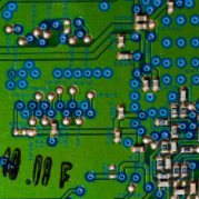
- reliability testing<\/a> to ensure zero design or manufacturing flaws.<\/li>\r\n\t<li><strong>Standardized Reference:<\/strong> Acts as a reference for <a href=https://www.nextpcb.com/"https:////www.nextpcb.com//blog//pcb-mass-production/">PCB mass production<\/a>, <a href=https://www.nextpcb.com/"https:////www.nextpcb.com//blog//what-is-pcb-testing/">PCB testing<\/a>, and PCB troubleshooting.<\/li>\r\n\t<li><strong>Authority: <\/strong>Typically confirmed for compliance by clients, design teams, or third-party certification bodies.<\/li>\r\n<\/ul>\r\n\r\n<p style=\"text-align: center;\"><img alt=\"\" src=https://www.nextpcb.com/"https:////www.nextpcb.com//uploads//images//202502//21//1740119124-0217-JbXFHC.png/" style=\"width: 800px; height: 533px;\" \/><\/p>\r\n\r\n<h3><strong>Golden Board vs First Article Inspection (FAI) <\/strong><\/h3>\r\n\r\n<p>In the PCB industry, Golden Board and First Article Inspection (FAI) are critical quality control concepts, but they differ significantly in terms of application scenarios, functional goals, and execution methods.<\/p>\r\n\r\n<table border=\"1\" cellpadding=\"1\" cellspacing=\"1\" style=\"width:700px;\">\r\n\t<tbody>\r\n\t\t<tr>\r\n\t\t\t<td><span style=\"color:#000000;\">Dimension<\/span><\/td>\r\n\t\t\t<td><span style=\"color:#000000;\"><strong>Golden Board<\/strong><\/span><\/td>\r\n\t\t\t<td><span style=\"color:#000000;\"><strong>First Article Inspection (FAI)<\/strong><\/span><\/td>\r\n\t\t<\/tr>\r\n\t\t<tr>\r\n\t\t\t<td><span style=\"color:#000000;\">Definition<\/span><\/td>\r\n\t\t\t<td><span style=\"color:#000000;\">Refers to a fully verified perfect sample used as a benchmark for production, testing, or design.<\/span><\/td>\r\n\t\t\t<td><span style=\"color:#000000;\">Refers to the full-dimensional inspection of the first completed product (or first batch of samples) before mass production.<\/span><\/td>\r\n\t\t<\/tr>\r\n\t\t<tr>\r\n\t\t\t<td><span style=\"color:#000000;\">Function<\/span><\/td>\r\n\t\t\t<td><span style=\"color:#000000;\">Calibrates equipment parameters, verifies testing procedures, defines acceptance criteria, or serves as a basis for quality agreements between customers and suppliers.<\/span><\/td>\r\n\t\t\t<td><span style=\"color:#000000;\">Verifies production processes, material compatibility, and design feasibility to ensure consistency in subsequent production.<\/span><\/td>\r\n\t\t<\/tr>\r\n\t\t<tr>\r\n\t\t\t<td><span style=\"color:#000000;\">Application Phase<\/span><\/td>\r\n\t\t\t<td><span style=\"color:#000000;\">After design finalization, used as a long-term reference standard.<\/span><\/td>\r\n\t\t\t<td><span style=\"color:#000000;\">Performed every time production is initiated or when process changes occur.<\/span><\/td>\r\n\t\t<\/tr>\r\n\t\t<tr>\r\n\t\t\t<td><span style=\"color:#000000;\">Verification Goal<\/span><\/td>\r\n\t\t\t<td><span style=\"color:#000000;\">Establishes design or testing benchmarks.<\/span><\/td>\r\n\t\t\t<td><span style=\"color:#000000;\">Verifies the compliance of the current production process.<\/span><\/td>\r\n\t\t<\/tr>\r\n\t\t<tr>\r\n\t\t\t<td><span style=\"color:#000000;\">Update Frequency<\/span><\/td>\r\n\t\t\t<td><span style=\"color:#000000;\">Updated only when design changes or standards are iterated.<\/span><\/td>\r\n\t\t\t<td><span style=\"color:#000000;\">Performed before every production batch.<\/span><\/td>\r\n\t\t<\/tr>\r\n\t\t<tr>\r\n\t\t\t<td><span style=\"color:#000000;\">Responsible Party<\/span><\/td>\r\n\t\t\t<td><span style=\"color:#000000;\">Usually provided by the designer or customer.<\/span><\/td>\r\n\t\t\t<td><span style=\"color:#000000;\">Executed by the manufacturer and inspection reports are submitted.<\/span><\/td>\r\n\t\t<\/tr>\r\n\t\t<tr>\r\n\t\t\t<td><span style=\"color:#000000;\">Inspection Scope<\/span><\/td>\r\n\t\t\t<td><span style=\"color:#000000;\">Focuses on overall performance and long-term stability.<\/span><\/td>\r\n\t\t\t<td><span style=\"color:#000000;\">Covers the comprehensiveness of processes, materials, and equipment parameters.<\/span><\/td>\r\n\t\t<\/tr>\r\n\t\t<tr>\r\n\t\t\t<td><span style=\"color:#000000;\">Example<\/span><\/td>\r\n\t\t\t<td><span style=\"color:#000000;\">In SMT (Surface-Mount Technology) assembly, the Golden Board may include standard solder pad shapes and component layouts, used to calibrate parameters for AOI (Automated Optical Inspection) equipment.<\/span><\/td>\r\n\t\t\t<td><span style=\"color:#000000;\">In PCBA (Printed Circuit Board Assembly) processing, the FAI requires passing visual inspection, functional testing, and environmental adaptability verification.<\/span><\/td>\r\n\t\t<\/tr>\r\n\t<\/tbody>\r\n<\/table>\r\n\r\n<p>In practical application, the Golden Board serves as a reference for the First Article Inspection (FAI), where it is used as a benchmark to assess whether the first article meets predefined quality standards. Conversely, the FAI validates the feasibility of the Golden Board when it is first put into production, ensuring its suitability in the actual manufacturing environment.<\/p>\r\n\r\n<h2><strong>Why Golden Board Matters in PCB Manufacturing?<\/strong><\/h2>\r\n\r\n<h4><strong>Design Verification & Optimization<\/strong><\/h4>\r\n\r\n<p>● Before PCB mass production, the Golden Board is used to validate design feasibility, including signal integrity (SI), power integrity (PI), thermal management, and mechanical structure.<\/p>\r\n\r\n<p>● Testing identifies potential issues (e.g., impedance mismatch, electromagnetic interference), guiding design optimization.<\/p>\r\n\r\n<h4><strong>Mass Production Benchmark<\/strong><\/h4>\r\n\r\n<p>● During PCB Mass production, the Golden Board serves as the "gold standard" for quality comparison, ensuring each batch of PCBs matches its performance, dimensions, materials, etc.<\/p>\r\n\r\n<p>● Helps pcb factories quickly detect manufacturing deviations (e.g., trace width errors, layer misalignment, soldering defects).<\/p>\r\n\r\n<h4><strong>Testing & Calibration<\/strong><\/h4>\r\n\r\n<p>● Calibrates testing equipment (e.g., flying probe testers, AOI systems) to ensure measurement accuracy.<\/p>\r\n\r\n<p>● In functional testing, the Golden Board acts as a "known good board" to validate the effectiveness of testing procedures.<\/p>\r\n\r\n<h4><strong>Issue Traceability<\/strong><\/h4>\r\n\r\n<p>● When faults occur during mass production, comparative analysis with the Golden Board allows for rapid pinpointing of the root cause (design defect vs. process defect).<\/p>\r\n\r\n<h2><strong>Production Process of Golden Board<\/strong><\/h2>\r\n\r\n<h4><strong>Design Phase<\/strong><\/h4>\r\n\r\n<p>● High-Precision Design: Layout and routing are completed using professional EDA tools (e.g., Altium, Cadence) to ensure compliance with electrical and mechanical specifications.<br \/>\r\n● Simulation Verification: Signal integrity, thermal, and EMI simulations to predict performance.<\/p>\r\n\r\n<h4><strong>Material Selection<\/strong><\/h4>\r\n\r\n<p>● Strict adherence to substrate materials (e.g., FR-4, Rogers HF materials), copper thickness, and surface finishes (e.g., ENIG, OSP).<\/p>\r\n\r\n<h4><strong>Small batch PCB Prototyping<\/strong><\/h4>\r\n\r\n<p>● Produced by experienced engineers in a controlled environment to avoid fluctuations from mass production equipment. High-precision equipment (e.g., laser drilling, LDI exposure machines) is used to ensure process consistency.<\/p>\r\n\r\n<h4><strong>Comprehensive Testing<\/strong><\/h4>\r\n\r\n<p>● Electrical Testing: Includes impedance testing, continuity testing (flying probe testing), and insulation resistance testing.<br \/>\r\n● Functional Testing: Actual power-on operation to verify signal transmission, power consumption, heat generation, etc.<br \/>\r\n● Reliability Testing: Accelerated aging experiments such as high-temperature and high-humidity tests, thermal cycling tests, and vibration tests.<\/p>\r\n\r\n<h4><strong>Certification and Sample Sealing<\/strong><\/h4>\r\n\r\n<p>● Jointly confirmed and signed by clients, design teams, and quality departments, archived as a legal reference for mass production.<\/p>\r\n\r\n<h2><strong>Key Applications of PCB Golden Boards<\/strong><\/h2>\r\n\r\n<ul>\r\n\t<li><strong>Telecommunications:<\/strong> High-frequency PCBs for 5G base stations and RF modules heavily rely on the Golden Board to ensure signal quality.<\/li>\r\n\t<li><strong>Automotive Electronics:<\/strong> Safety-critical ECUs validated for reliability.<\/li>\r\n\t<li><strong>Consumer Electronics: <\/strong>Miniaturized PCBs for mobile phone motherboards and wearable devices depend on the Golden Board for layout optimization.<\/li>\r\n\t<li><strong>Military\/Aerospace:<\/strong> PCBs in extreme environments undergo extreme condition testing validated by the Golden Board.<\/li>\r\n<\/ul>\r\n\r\n<h2><strong>Golden Board vs. Mass-Produced PCBs: Key Differences<\/strong><\/h2>\r\n\r\n<table border=\"1\" cellpadding=\"1\" cellspacing=\"1\" style=\"width:700px;\">\r\n\t<tbody>\r\n\t\t<tr>\r\n\t\t\t<td><span style=\"color:#000000;\">Aspect<\/span><\/td>\r\n\t\t\t<td><span style=\"color:#000000;\"><strong>Golden Board<\/strong><\/span><\/td>\r\n\t\t\t<td><span style=\"color:#000000;\"><strong>Mass-Produced PCBs<\/strong><\/span><\/td>\r\n\t\t<\/tr>\r\n\t\t<tr>\r\n\t\t\t<td><span style=\"color:#000000;\">Purpose<\/span><\/td>\r\n\t\t\t<td><span style=\"color:#000000;\">Design validation, benchmarking<\/span><\/td>\r\n\t\t\t<td><span style=\"color:#000000;\">Volume production, end-use<\/span><\/td>\r\n\t\t<\/tr>\r\n\t\t<tr>\r\n\t\t\t<td><span style=\"color:#000000;\">Production<\/span><\/td>\r\n\t\t\t<td><span style=\"color:#000000;\">Low-volume, precision-controlled<\/span><\/td>\r\n\t\t\t<td><span style=\"color:#000000;\">High-volume, process variations<\/span><\/td>\r\n\t\t<\/tr>\r\n\t\t<tr>\r\n\t\t\t<td><span style=\"color:#000000;\">Testing<\/span><\/td>\r\n\t\t\t<td><span style=\"color:#000000;\">Full validation (electrical + functional + reliability)<\/span><\/td>\r\n\t\t\t<td><span style=\"color:#000000;\">Sampling (e.g., AOI, flying probe)<\/span><\/td>\r\n\t\t<\/tr>\r\n\t\t<tr>\r\n\t\t\t<td><span style=\"color:#000000;\">Cost<\/span><\/td>\r\n\t\t\t<td><span style=\"color:#000000;\">High (iterations, exhaustive tests)<\/span><\/td>\r\n\t\t\t<td><span style=\"color:#000000;\">Low (economies of scale)<\/span><\/td>\r\n\t\t<\/tr>\r\n\t<\/tbody>\r\n<\/table>\r\n\r\n<h2><strong>Importance Summary<\/strong><\/h2>\r\n\r\n<p>● <strong>Risk Control: <\/strong>Prevents production failures due to design defects, reducing economic losses.<br \/>\r\n●<strong> Efficiency Improvement: <\/strong>Shortens product development cycles through standardized processes.<br \/>\r\n●<strong> Quality Consistency:<\/strong> Ensures stable performance of mass-produced products, meeting industry standards (e.g., IPC-A-600).<br \/>\r\nThe Golden Board serves as a vital bridges between PCB design, PCB manufacturing, and quality control in the PCB industry, making it indispensable, especially in high-end electronics sectors that demand high frequency, high density, and high reliability.<\/p>\r\n","status":1,"create_time":1745740824,"update_time":1745740859,"clicks":766,"hits":0,"custom_url":"what-is-a-golden-board-in-pcb","related":"","add_uid":36,"publish_uid":0,"attr":0,"type":0,"keywords":"","comment_count":0,"share_count":0,"need_move":0,"c_time":"2025-04-27 16:00:24","u_time":"2025-06-27 16:13:33","comments_count":0,"is_like":0}">
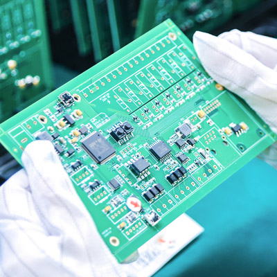
-

- Deploy Smarter IoT solutions with SIM7600 4G LTE Modules and Free Prototypes - NextPCB Accelerator #7<\/a><\/p>\r\n","status":1,"create_time":1743133410,"update_time":1743575914,"clicks":1766,"hits":1,"custom_url":"simcom-sim7600","related":"","add_uid":36,"publish_uid":0,"attr":0,"type":0,"keywords":"","comment_count":0,"share_count":0,"need_move":0,"c_time":"2025-03-28 11:43:30","u_time":"2025-06-27 14:54:56","comments_count":0,"is_like":0}">
-


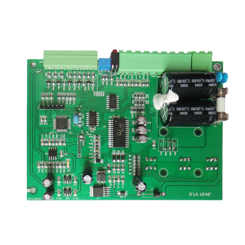
Categories
Recommended Article:
- Quick Turn PCB Manufacturer: Your Reliable Partner for Urgent Projects -NextPCB
- Prevent PCB Insulation Failure: PP Thickness & Stackup Guide
- Best 6-Layer PCB Stackups for Signal Integrity & Impedance Control
- SMT Red Glue: Why It’s Used & How to Optimize for Cost-Effective PCB Assembly
- How to Select the Optimal PCB Hole Size for Through-Hole Pins (Avoid Assembly Failures!)
- Get Early Access to Raspberry Pi RP2354 MCU with NextPCB - NextPCB Accelerator #11
- How to Achieve 50 Ohm Impedance Requirements for PCB Routing without extra charges
- HQDFM PCB Design Analysis Tool User Manual
- Fast Turn Low Volume PCB Assembly Services from China: Speed, Quality & Cost-Efficiency
- NextPCB Lands on Crowd Supply: Supercharging Hardware Startups from Prototype to Production
