
 PCB Assembly
 Layer Buildup
 Online Tools
 PCB Design-Aid & Layout
 Mechanics
 SMD-Stencils
 Quality
 Drills & Throughplating
 Factory & Certificate
 PCB Assembly Factory Show
Certificate
PCB Assembly Factory Show
Certificate
Support Team
Feedback:
support@nextpcb.comForget theory – impedance control in your 6-layer PCB stackup directly determines if your high-speed signals actually work. Get it wrong with a common 1.6mm board thickness and 1oz copper thickness, and reflections trash your signal integrity. Think jitter, data errors, and failed compliance tests. It’s why experienced designers constantly wrestle with the core question: "How do I arrange this 6-layer stackup for precise impedance?"
The problem? Squeezing planes and signals into that fixed 1.6mm height while hitting targets like 50Ω/90Ω. Random layer ordering makes controlled impedance nearly impossible using practical trace widths. A bad stack guarantees tuning nightmares or a dead board. This guide cuts through that – showing you an optimized layer arrangement that makes impedance predictable, ensuring your design performs reliably, not just on paper.
6-layer board, 1.6mm board thickness, 1oz copper thickness, how to arrange the stackup to achieve the best impedance effect?
The laminate structure recommended to customers:Board Thickness = 1.6mm
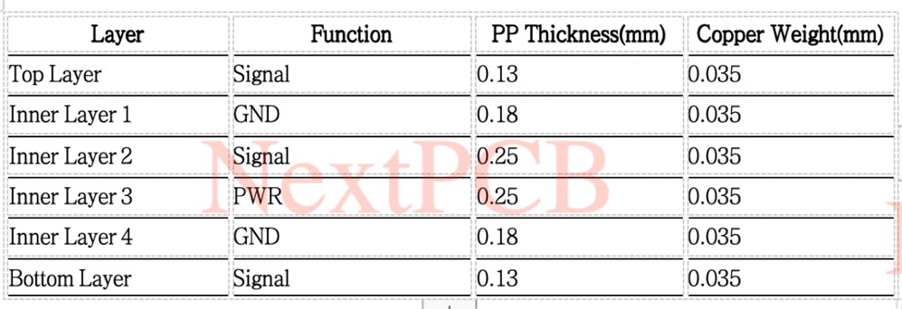
The PWR layer is placed in the middle, forming a plane pair with the upper and lower GND Planes, which plays a distributed decoupling role and reduces power noise and electromagnetic radiation.
The copper content, dielectric thickness, and reference surface distribution of the upper and lower signal layers are symmetrical to ensure processing and assembly stability.
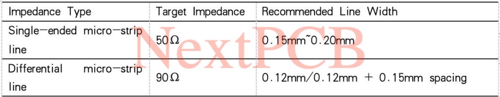
Impedance Target Recommendations: 50Ω Single-Ended & 90Ω Differential
Want to learn more? We have a dedicated article on PCB impedance. Also have practical tutorial regarding How to Achieve 50 Ohm Impedance Requirements for PCB Routing without extra charges. If your design has other impedance control requirements, feel free to reach out to our tech team anytime for support.
Still, need help? Contact Us: support@nextpcb.com
Need a PCB or PCBA quote? Quote now
|
Dimensions: (mm) |
|
|
Quantity: (pcs) |
|
|
Layers: |
Thickness: |
 Quote now
|
|

 Printed Circuit Boards
 Surface

