Printed Circuit Boards
 Surface
 PCB Assembly
 Layer Buildup
 Online Tools
 PCB Design-Aid & Layout
 Mechanics
 SMD-Stencils
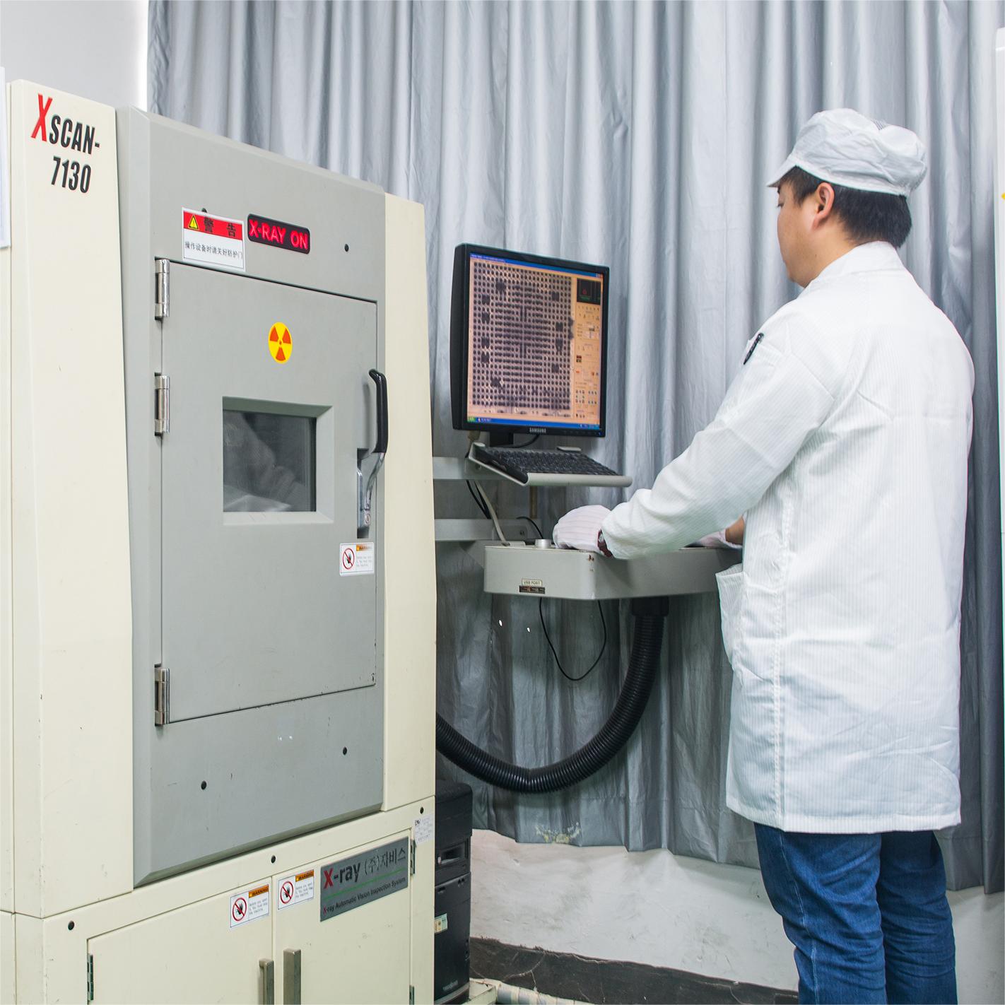
 Quality
 Drills & Throughplating
 Factory & Certificate


-

-
-
-
-
-
-
-
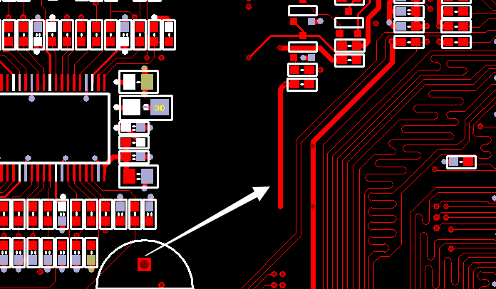
Introduction to Via in Pad Technology
Introducing pcb pad holes and designing it precautions
3188 1 0 Shares
-
-
-
-
-
-
-
-
-
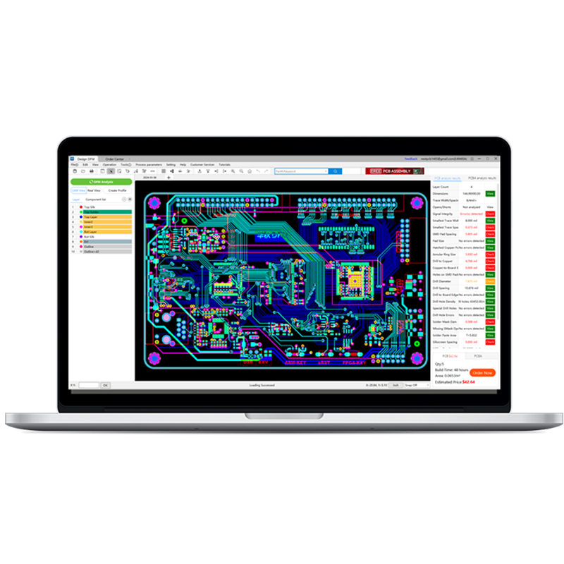
DFM, DFMA, DFA. Part 2. NextPCB's PC program
Detailed example of using the desktop version of HQDFM.
3161 2 0 Shares
-
-
-
DFM, DFMA, DFA. Part 1. Kicad and Online Gerber Viewer
The comparison of KiCad Gerber Viewer and HQ PCB DFM Gerber Viewer.
3302 2 0 Shares
Categories
Recommended Article:
- Quick Turn PCB Manufacturer: Your Reliable Partner for Urgent Projects -NextPCB
- Prevent PCB Insulation Failure: PP Thickness & Stackup Guide
- Best 6-Layer PCB Stackups for Signal Integrity & Impedance Control
- SMT Red Glue: Why It’s Used & How to Optimize for Cost-Effective PCB Assembly
- How to Select the Optimal PCB Hole Size for Through-Hole Pins (Avoid Assembly Failures!)
- Get Early Access to Raspberry Pi RP2354 MCU with NextPCB - NextPCB Accelerator #11
- How to Achieve 50 Ohm Impedance Requirements for PCB Routing without extra charges
- HQDFM PCB Design Analysis Tool User Manual
- Fast Turn Low Volume PCB Assembly Services from China: Speed, Quality & Cost-Efficiency
- NextPCB Lands on Crowd Supply: Supercharging Hardware Startups from Prototype to Production