Printed Circuit Boards
 Surface
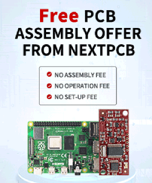
 PCB Assembly
 Layer Buildup
 Online Tools
 PCB Design-Aid & Layout
 Mechanics
 SMD-Stencils
 Quality
 Drills & Throughplating
 Factory & Certificate


-
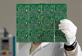
PCB layout problems
First, consider the size of the PCB.
4050 1 0 Shares
-
-
-
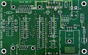
How to design Multilayer PCB
Multi-layer and double-sided PCB design is similar, and even easier.
4215 1 0 Shares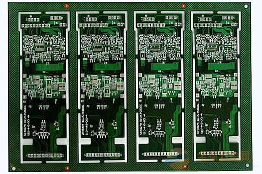
-
-

-
-
-
-
-
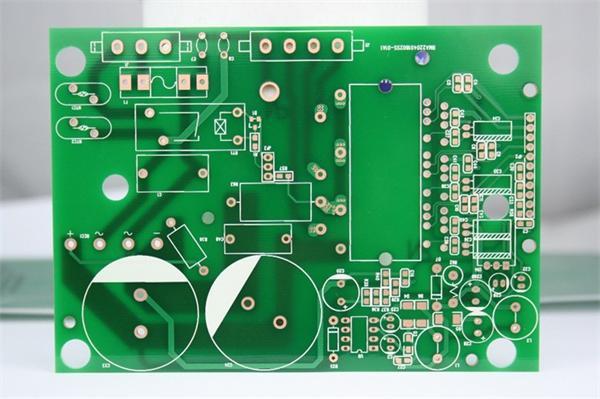
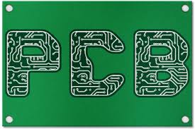
The meaning of those letters on the PCB
Rx:the resistance, a lot of resistance in the circuit diagram, according to theserial number, R1, R2...
5304 3 0 Shares
-
PROTEL commonly used shortcuts
PageUp:Zoom in with the mouse
4900 3 0 Shares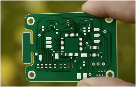
Categories
Recommended Article:
- Quick Turn PCB Manufacturer: Your Reliable Partner for Urgent Projects -NextPCB
- Prevent PCB Insulation Failure: PP Thickness & Stackup Guide
- Best 6-Layer PCB Stackups for Signal Integrity & Impedance Control
- SMT Red Glue: Why It’s Used & How to Optimize for Cost-Effective PCB Assembly
- How to Select the Optimal PCB Hole Size for Through-Hole Pins (Avoid Assembly Failures!)
- Get Early Access to Raspberry Pi RP2354 MCU with NextPCB - NextPCB Accelerator #11
- How to Achieve 50 Ohm Impedance Requirements for PCB Routing without extra charges
- HQDFM PCB Design Analysis Tool User Manual
- Fast Turn Low Volume PCB Assembly Services from China: Speed, Quality & Cost-Efficiency
- NextPCB Lands on Crowd Supply: Supercharging Hardware Startups from Prototype to Production