Printed Circuit Boards
 Surface
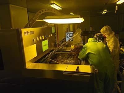
 PCB Assembly
 Layer Buildup
 Online Tools
 PCB Design-Aid & Layout
 Mechanics
 SMD-Stencils
 Quality
 Drills & Throughplating
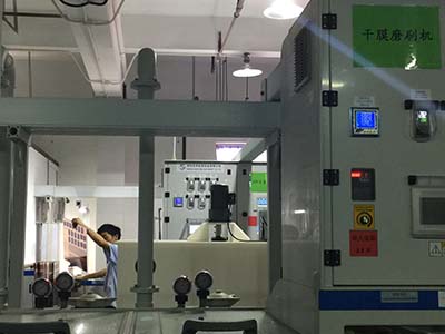
 Factory & Certificate


-
-
Two major problems in high speed PCB design
1. EMC, EMI. 2. Routing skills for high-speed differential signals
3136 1 0 Shares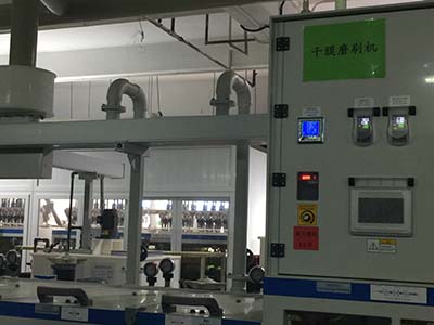
-

-
-
-
-
Method of avoiding transmission line effects
The ways to control the effects of transmission line effects from the following aspects.
3066 2 0 Shares
-
-
-
-
Analysis of problems in PCB design (16-25)
Can you introduce some foreign technical books and materials on high-speed PCB design?
3163 7 0 Shares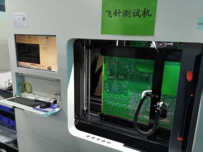
-
-
-
-
-
-
-
-
-
Categories
Recommended Article:
- Quick Turn PCB Manufacturer: Your Reliable Partner for Urgent Projects -NextPCB
- Prevent PCB Insulation Failure: PP Thickness & Stackup Guide
- Best 6-Layer PCB Stackups for Signal Integrity & Impedance Control
- SMT Red Glue: Why It’s Used & How to Optimize for Cost-Effective PCB Assembly
- How to Select the Optimal PCB Hole Size for Through-Hole Pins (Avoid Assembly Failures!)
- Get Early Access to Raspberry Pi RP2354 MCU with NextPCB - NextPCB Accelerator #11
- How to Achieve 50 Ohm Impedance Requirements for PCB Routing without extra charges
- HQDFM PCB Design Analysis Tool User Manual
- Fast Turn Low Volume PCB Assembly Services from China: Speed, Quality & Cost-Efficiency
- NextPCB Lands on Crowd Supply: Supercharging Hardware Startups from Prototype to Production