Printed Circuit Boards
 Surface
 PCB Assembly
 Layer Buildup
 Online Tools
 PCB Design-Aid & Layout
 Mechanics
 SMD-Stencils
 Quality
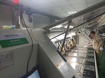
 Drills & Throughplating
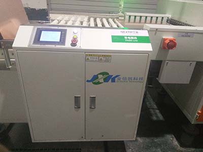
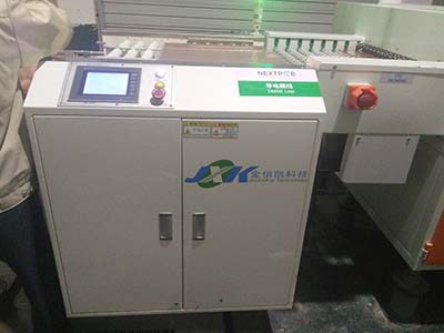
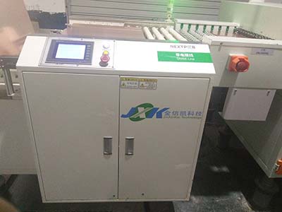
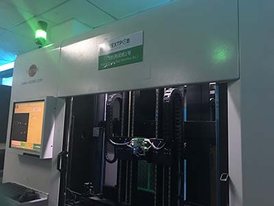
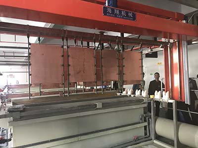
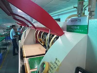
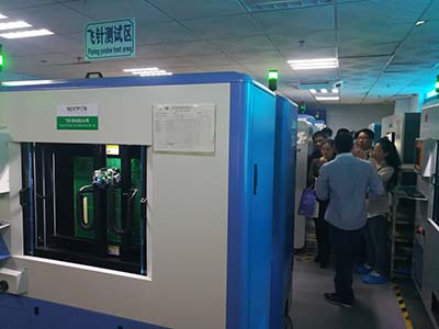
 Factory & Certificate


-

-
Tips and methods for high frequency PCB design
1. The corner of the transmission line should be at a 45° angle to reduce the return loss.
2985 1 0 Shares
-
Several issues that should be taken seriously by mobile phone PCB design
1. Power and ground processing
3168 1 0 Shares
-
How to ensure that no noise is added when designing PCB
It must be considered from the following aspects:
2990 1 0 Shares
-
RF layout tips for mobile phone PCB design
The increase in the functionality of the mobile phone requires higher design of the PCB.
3008 1 0 Shares
-
PCB design tips 100, teach you to master PCB design easily (25-30)
In this article, we will teach you how to do a PCB design easily 25-30
3224 3 0 Shares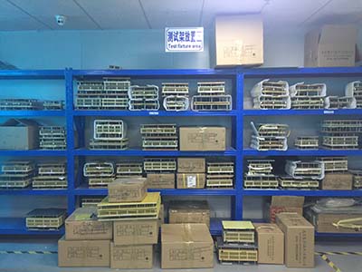
-

-
-
-
-
PCB Design Process - Introduction to DFM
Allow enough test interfaces to facilitate ICT testing
3589 1 0 Shares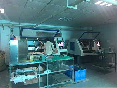
-
-
PCB layout and system test
The basic principles of high-speed PCB layout are as follows:
3640 1 0 Shares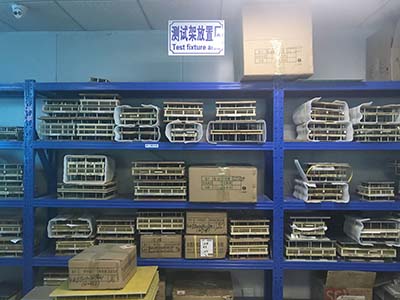
-
-
-
-

-
-
-
Checking List After Drawing a Package
(1) Is the pin pitch correct? If the answer is no, it is very likely that you will not even get a weld.
3229 4 0 Shares
Categories
Recommended Article:
- Quick Turn PCB Manufacturer: Your Reliable Partner for Urgent Projects -NextPCB
- Prevent PCB Insulation Failure: PP Thickness & Stackup Guide
- Best 6-Layer PCB Stackups for Signal Integrity & Impedance Control
- SMT Red Glue: Why It’s Used & How to Optimize for Cost-Effective PCB Assembly
- How to Select the Optimal PCB Hole Size for Through-Hole Pins (Avoid Assembly Failures!)
- Get Early Access to Raspberry Pi RP2354 MCU with NextPCB - NextPCB Accelerator #11
- How to Achieve 50 Ohm Impedance Requirements for PCB Routing without extra charges
- HQDFM PCB Design Analysis Tool User Manual
- Fast Turn Low Volume PCB Assembly Services from China: Speed, Quality & Cost-Efficiency
- NextPCB Lands on Crowd Supply: Supercharging Hardware Startups from Prototype to Production